Under conditions where a CCD is exposed to very high intensity illumination, it is possible to exhaust the storage capacity of the CCD wells, a condition known as blooming. When this occurs, excess charge will overflow into adjacent CCD photodiode wells resulting in a corrupted image near the blooming site.
The size of a pixel charge accumulation well is determined by the photodiode area, which is filled with electrons in a linear relationship dependent on the amount of light incident upon the photodiode. As the pixel well nears the saturation limit (becomes filled with electronic charge), this linear relationship fails and the pixel's response to additional illumination decreases, causing degradation of the signal. The point at which the photometric response to illumination deviates from linearity is termed a linear full well, and is usually the size of the signal necessary to satisfy the bit depth of the analog-to-digital converter. Prior to saturation, random noise (determined by the square root of the signal) is reduced by a condition known as noise clipping.
CCD Blooming
Explore how a laterial overflow drain operates to remove excess integrated charge from CCD potential wells.
When saturated, additional charge generated by light on the photodiode spills over to adjacent pixel wells, which will also become saturated and report erroneously high illumination levels. Because pixel wells can integrate more charge than they can effectively transfer, saturation occurs when the maximum well-transfer capacity is reached. Under conditions where the entire photodiode array is saturated, or during periods of extensive serial and parallel shift register binning, the output node may also become saturated and cause the output sequence to collapse, resulting in total signal loss. Blooming is manifested by white streaks that totally wash out any details of the image.
In many cases, blooming can be minimized by decreasing charge integration time, but this remedy is not always successful so additional mechanisms to drain excess charge have been developed. Clocking schemes have also been devised to control pixel blooming during integration. The most common clocking approach involves alternate switching of clock-voltage phases to force excess charge into the barrier region nested between the CCD silicon substrate and oxide layer, where it is recombined with electron "holes" in the crystalline silicon lattice. Clock voltage switching selectively bleeds off excess charge without compromising image information in pixels that are not yet saturated. This technique has been termed clocked anti-blooming, and is useful in low-light level scientific applications, such as fluorescence microscopy, but suffers from reduced efficiency at high frame rates.
A more common anti-blooming technique involves "overflow" drain structures that are incorporated into the CCD during fabrication. Two of the most common drain structures are the vertical overflow drain (VOD) and the lateral overflow drain (LOD). Drains enable integration time to be controlled independently of charge readout, which allows them to serve as an electronic exposure or shutter mechanism to limit pixel saturation and provide a more reliable shuttering method than is currently possible with mechanical devices.
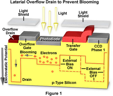
During CCD fabrication, a new gate is established adjacent to the photodiode called the pixel reset gate or the overflow gate (see Figure 1). This gate allows excess charge to be shunted from the photodiode to a common drain without affecting the CCD signal. Figure 1 illustrates a typical lateral overflow drain structure that manufacturers incorporate into high-performance CCD architectures. Excess charge collected by the photodiode is allowed to spill (via the overflow gate) into the drain, which is a reversed-biased diode that removes the charge to ground. Many CCD designs incorporate lateral drains that run the length of the parallel shift register and are shared by all pixel gates. In contrast, vertical overflow drains are positioned in the charge accumulation site and have an electrostatic potential barrier that is limited to allow excess charge to overflow directly into the silicon substrate. The primary drawback of the lateral overflow gate is a reduced quantum efficiency manifested in a reduced charge handling capacity, which leads to a less sensitive photo response.