Full-frame charge-coupled devices (CCDs) feature high-density pixel arrays capable of producing digital images with the highest resolution currently available. This popular CCD architecture has been widely adopted due to the simple design, reliability, and ease of fabrication.
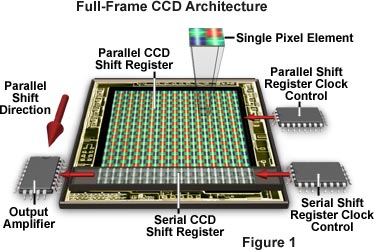
The pixel array illustrated in the full-frame CCD drawing presented in Figure 1 consists of a parallel shift register, onto which images are optically projected by means of a camera lens or microscope optical train. In this configuration, all of the photodiodes in the pixel array collectively act as the image plane and are available for detecting photons during the exposure period. A miniature portion of the total image is contained in each pixel element, which consists of four photodiodes masked with red, green, and blue colored filters. The image presented in the upper portion of Figure 1 is an actual high-magnification photomicrograph of a single pixel element.
Full-Frame CCD Operation
Explore how images are formed, then transferred in a parallel manner to the serial horizontal shift register.
After photons composing the image have been collected by the pixel elements and converted into electrical potential, the CCD undergoes readout by shifting rows of image information in a parallel fashion, one row at a time, to the serial shift register (illustrated as a series of gray-scale elements at the bottom of the pixel array). The serial register then sequentially shifts each row of image information to an output amplifier as a serial data stream. All integrated charge must be clocked out of the serial register before the next parallel line of image data can be transferred to the horizontal array. The entire process is repeated until all rows of image data have been directed to the output amplifier and off the chip to a analog-to-digital signal converter integrated circuit. Reconstruction of the image in a digital format yields the final photograph or photomicrograph.
Full-frame CCD architecture has what is termed a 100 percent fill factor, meaning that the entire pixel array is used to detect incoming photons during exposure to the object being imaged. Full-frame pixel array sizes are often based upon powers of 2 (512 × 512, 768 × 768, or 1024, × 1024 pixels) to simplify memory mapping of the array and image processing algorithms. CCDs of this type typically have square pixel dimensions to avoid image distortion and are fabricated with pixel sizes ranging from 7 to 24 microns in arrays containing up to 6 million pixels. Due to the fact that the pixel array is used for both image detection and readout, a mechanical shutter or synchronized strobe illumination scheme must be used to prevent smearing for most exposure periods. Smear occurs when the photodiodes are continuously illuminated during parallel register readout, and will be oriented in the direction of charge transport through the parallel array. In Fluroescence microscopy, where image integration time greatly exceeds the register readout rate, smear may become insignificant.
Image data transfer rates are limited by the output amplifier bandwidth and the conversion speed of the analog-to-digital converter. Readout rates can be dramatically increased by subdividing the pixel array into smaller, but identical sub-arrays, which can then be read simultaneously. Image reconstruction is then performed by an external video processor circuit that collects, decodes, and reformats the original image.
Both frontside and backside illumination schemes have been successfully utilized with full-frame CCD architecture, although devices illuminated from the back typically provide a higher quantum transfer yield. Incoming photons are converted to electrical charge (integrated) with greater efficiency because light enters the CCD silicon substrate from the rear, circumventing the necessity to pass through semiconductor gate areas that blanket the light-sensitive photodiodes. Recently, new CCD technologies have been introduced that apply materials such as indium tin oxide to gate fabrication in an effort to render the gates more sensitive to light, helping to raise the quantum efficiency and eliminating the need for backside illumination.