An important characteristic of a scientific imaging system is the linearity in response to incident light, particularly when applied for quantitative photometric analysis. In digital camera systems employing charge-coupled device (CCD) sensors, the fundamental function of the CCD is to convert photons carrying image information into an electronic signal. After digitization, the signal output should ideally be linearly proportional to the amount of light incident on the sensor.
A transfer function relating the number of photons incident on the sensor and the digital output is determined by a multi-stage process that begins with the creation and transfer of charge carriers (electron-hole pairs) in the active pixel regions, followed by conversion of electrons from the charge domain into the voltage domain as an amplified voltage signal. This analog signal passes through a series of processing steps, and is further amplified before finally being digitized for display, image processing, and storage. With proper device design, the transfer function results in a linear variation of final digitized output signal in relation to the amount of light incident on the CCD, such that the output signal is equal to the photon input multiplied by a proportionality constant.
Significant differences exist in the methods utilized by various manufacturers to measure and report CCD linearity. A common technique for assessing linearity is based on a graphical plot of measured output signal as a function of exposure time, extending to the full well capacity of the device (the number of electrons held by a potential well or pixel; also referred to as linear full well). The specification may be defined as a percentage of deviation from linearity in comparison to the maximum signal intensity obtained at full well conditions. Note that the same measurement may be reported by different manufacturers as either linearity or nonlinearity.
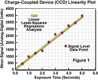
Calculation of the deviation from linearity begins with the plot of signal level versus exposure (integration) time. The signal level is typically specified as a number of counts, or as a relative digital number (DN) or an "ADC unit" (ADU), which is a value output by the analog-to-digital converter that is proportional to voltage. Figure 1 illustrates a linearity plot of this type for a high-performance CCD. A linear least-squares regression analysis is fit to the data, and the deviation for each data point from the calculated best-fit line is determined in order to identify the maximum positive and negative deviation values. The nonlinearity, as a percentage, is calculated as follows, in which the absolute value is used for both deviation maxima:
The linearity of a camera system is determined by the CCD itself, as well as other electronic components in the signal processing chain, culminating with the analog-to-digital converter. In effect, any nonlinearity indicates a change in the camera's gain constant with signal level. Quantitative imaging operations, such as arithmetic ratio determinations, linear transformations, shading corrections, and other processing algorithms rely on absolute signal measurements, and require that there be no significant interdependence between camera gain and signal intensity. High-performance CCD imaging systems exhibit extremely good linearity over a wide signal range compared to most other imaging sensors, including film, vidicon tubes, and video CCD cameras, which may deviate from linearity by several percent. CCD cameras intended for scientific use commonly have nonlinearity values in the range of a few tenths of one percent over a signal range of 4 or 5 orders of magnitude. The deviations from linearity are typically constant, and if well characterized, the nonlinearity can be corrected through lookup tables to a value of less than one-tenth of a percent.
Although CCD sensors respond in a linear manner over a wide dynamic range, when full well conditions are reached under high average illumination intensity, a nonlinear response is usually observed. Note that good linearity may extend beyond full well in situations where a small region of the image field is overexposed, but is surrounded by a lower average intensity level. If overall illumination is sufficiently bright, the CCD response becomes nonlinear and saturation occurs, accompanied by blooming (charge overflow from pixels exceeding full well capacity) over the entire array. Saturation exists when an increase in intensity produces no further change in recorded signal. With excessive average intensity over the entire pixel array, the onset of nonlinear response and full well capacity occur at the same signal level.
Depending upon the sensor characteristics, nonlinear response may also result under extremely low illumination levels, and in principle, the response in the nonlinear regions can be calibrated if necessary. The best practice, however, is to limit exposures to the region of linearity for the particular sensor being utilized, since the onset of saturation can be rapid and difficult to predict. Among the measures that can be taken to avoid CCD saturation in high illumination conditions is to capture several shorter exposures that are equivalent in duration to the desired longer integration interval. The multiple short-exposure images can be combined during processing, although in some applications consideration must be given to the implications of the different signal-to-noise factors that prevail when combining short exposures compared to a single exposure integration over a longer interval.