In modern widefield fluorescence and laser scanning confocal optical microscopy, the collection and measurement of secondary emission gathered by the objective can be accomplished by several classes of photosensitive detectors, including photomultipliers, photodiodes, and solid-state charge-coupled devices (CCDs). In confocal microscopy, fluorescence emission is directed through a pinhole aperture positioned near the image plane to exclude light from fluorescent structures located away from the objective focal plane, thus reducing the amount of light available for image formation. As a result, the exceedingly low light levels most often encountered in confocal microscopy necessitate the use of highly sensitive photon detectors that do not require spatial discrimination, but instead respond very quickly with a high level of sensitivity to a continuous flux of varying light intensity.
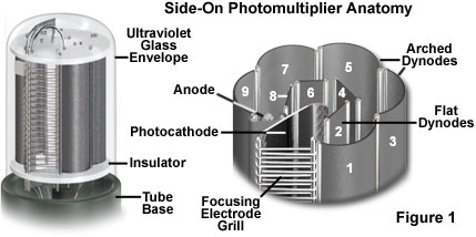
Photomultipliers, which contain a photosensitive surface that captures incident photons and produces a stream of photoelectrons to generate an amplified electric charge, are the popular detector choice in many commercial confocal microscopes. These detectors contain a critical element, termed a photocathode, capable of emitting electrons through the photoelectric effect (the energy of an absorbed photon is transferred to an electron) when exposed to a photon flux. The general anatomy of a photomultiplier (illustrated in Figure 1) consists of a classical vacuum tube in which a glass or quartz window encases the photocathode and a chain of electron multipliers, known as dynodes, followed by an anode to complete the electrical circuit. When the photomultiplier is operating, current flowing between the anode and ground (zero potential) is directly proportional to the photoelectron flux generated by the photocathode when it is exposed to incident photon radiation.
Photocathodes are fabricated using either alkali metals or semiconductors, and are designed to respond to a wavelength region dictated by the composition of the base material utilized in the construction. Sensitivity to the wavelength of incident illumination is referred to as the spectral response or the responsivity (R) of a photocathode, and is described by the equation:
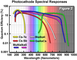
where q is the charge of an electron, QE is the quantum efficiency of the photosensitive surface, h is Planck's constant, and c is the speed of light. The quantum efficiency of a detector is a measure of the fraction of incident photons that result in a detectable output from the photosensor. The photocathode composition determines not only the spectral response of a photomultiplier, but also the quantum efficiency at each wavelength, the overall uniformity of photomultiplier sensitivity, and the dark current (discussed below). Figure 2 presents spectral response curves for a variety of typical photomultiplier photocathodes, as well as the quantum efficiency for each cathode, calculated from the responsivity for each material. Even the best photocathodes that respond to light in the visible region of the spectrum are less than 30-percent quantum efficient. This means that 70 percent of the photons that impact on the photocathode surface do not produce a photoelectron and are, therefore, not detected.
As is evident in Figure 2, most photocathode materials have good response in the shorter wavelength regions of the visible and ultraviolet spectrum, between approximately 200 and 400 nanometers. Photomultipliers that have photocathodes composed of bialkali materials have a higher quantum efficiency and lower noise level in the green region of the spectrum (550-nanometers), while those with multialkali photocathodes respond better in the red and near-infrared. Bialkali photocathodes are composed of an alloy containing antimony and several alkali metals, such as rubidium, potassium, and cesium. The spectral response of bialkali photocathodes is excellent in the ultraviolet and blue regions, but drops quickly as visible wavelengths stretch into the green and red regions. Multialkali photocathodes (often referred to as S20) are composed of similar materials, but with the addition of at least three alkali metals, and have a wider spectral response region that extends into the red and near-infrared portions.
Even with their superior gain characteristics, photomultipliers have some disadvantages when compared to other types of detectors. The gain and dark current performance of individual photomultipliers from the same production run can vary widely, often by a factor of 2 to 5 for a particular design. In addition, the devices can be damaged by exposure to high illumination levels, often requiring very long recovery times (some never recover from high intensity illumination). Modern photocathodes yield very good visible and ultraviolet performance, but sensitivity drops dramatically in the longer visible wavelengths and infrared. Photomultipliers require a stabilized high voltage power supply, which increases the cost of using these detectors. Finally, even in the most sensitive wavelength region, about two-thirds of the incident light is not detected by the photocathode and does not contribute to photomultiplier gain.
In operation, incident photons pass through the photomultiplier window and impact on the photocathode surface to subsequently generate photoelectrons that are ejected into the vacuum. Absorbed photons produce a free electron in the photocathode and the surplus energy is converted into kinetic energy. Electrons having sufficient kinetic energy are able to escape from the photocathode surface. These emitted photoelectrons are controlled by a focusing electrode, which directs the stream to the first element in the chain of dynodes (consisting of up to 18 elements) that serves to multiply electrons through a secondary emission process. The focusing electrodes are usually present to ensure that photoelectrons emitted near the edges of the photocathode will be likely to impact on the surface of the first dynode. In addition, an electrical potential of approximately 100 volts is applied between the photocathode and the first dynode element in the chain. The impact of a photoelectron on the first dynode releases additional electrons (usually between 5 and 10) that are accelerated in turn toward the next dynode, which also has a potential difference of about 100 volts with respect to the first. Each electron produces several more secondary electrons that continue to flow down the chain from one dynode to the next with the same potential difference of 100 volts between the dynodes. Thus, the dynodes serve as electron multipliers by virtue their geometry and the gradation in voltage between the individual elements.
As the secondary electrons travel down the dynode chain, they are amplified and ultimately collected by the anode as an output signal. The electron multiplication capabilities of the dynode chain are quite impressive. Electron gains of 10 million are possible if 12 to 14 dynodes stages are employed. However, total gain varies with the voltage applied across the dynode chain and with the number of dynodes. Because of the high level of electron multiplication by the dynode chain (gain), photomultiplier detectors provide extremely high sensitivity to light and have exceptionally low noise when compared to other photosensitive devices. The gain of a photomultiplier can be estimated using the following equation:
where µ is the current amplification (gain), δ is the secondary emission ratio for the dynodes, and n is the number of dynode stages. For example, in a 10-stage photomultiplier with a secondary emission ratio of five, the current amplification would be about 10 million. As an added benefit, high gain is achieved without sacrificing bandwidth, and high-end photomultipliers can be designed with bandwidths in the range of 1 to 1.5 gigahertz (although 100 megahertz is more common for the photomultipliers used in confocal microscopy). In addition, photomultipliers feature a very fast response time and are versatile with regards to size limitations on the photocathode. These characteristics make the photomultiplier an ideal detector for the low light levels frequently encountered with weakly emitting fluorophores in laser scanning confocal microscopy.
The physical arrangement of the dynode chain varies according to the mechanical requirements for the size and geometry of the photomultiplier. Dynodes have a surface composed of beryllium-copper or antimony-cesium, depending upon the application. Beryllium-copper is preferred for fast pulse measurements, particularly where a linear response is critical. On the other hand, antimony-cesium dynodes exhibit higher gain than beryllium-copper dynodes and require lower operating voltages, but their time response varies with the applied voltage across the dynode chain. Upon exiting the dynode chain, the pulse of multiplied electrons is collected on the anode, which usually has a potential difference of approximately 1000 volts with respect to the photocathode. Photomultipliers are usually operated from a negative high voltage, with the cathode at the most negative potential and each successive dynode biased at a slightly less negative potential. The anode voltage is close to ground potential. By carefully matching dynode shape and proximity to the large interspersed electric fields, the output pulse on the anode can be reduced to several nanoseconds in duration to preserve the temporal profile of the initial optical signal. Current pulses ranging up to 100 microamperes from a single photon can be achieved in high-gain photomultipliers, a level that can easily be detected without further amplification.
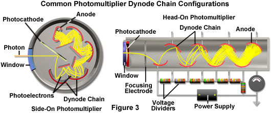
The two most popular photomultiplier designs have configurations that place the sensitive photocathode element either at the end (head-on) or on the side (side-on) of the vacuum tube (see Figure 3). Incident light is detected through a window at the top of the glass envelope in head-on designs, and through the curved side in side-on photomultipliers. Due to their high performance ratings and low cost, side-on photomultipliers are the most widely used tubes for general photometric applications, such as spectrophotometry, fluorimetry, and confocal microscopy. Side-on photomultipliers contain an opaque and relatively thick reflection-mode photocathode surrounded by a circular cage-like dynode element chain. Incident photoelectrons do not pass through the photocathode in a side-on photomultiplier, but instead are ejected from the front face and angled toward the first dynode element.
In contrast, the photocathode in an end-on photomultiplier must be of precise thickness as well as composition, and is semi-transparent. The photoemissive material is deposited on the surface of an optical window so that electrons are emitted from the side of the photocathode opposite that of the incident radiation. If the photocathode is too thick, more photons will be absorbed but fewer photoelectrons will be emitted from the rear surface. Alternatively, if the photocathode is too thin, photons may pass straight through without being absorbed. Because of these differences in design, side-on photomultipliers having photocathodes of similar composition to head-on tubes often exhibit higher quantum efficiencies.
Channel photomultipliers represent a new design that incorporates a unique detector having a semitransparent photocathode deposited onto the inner surface of the entrance window. Photoelectrons released by the photocathode enter a narrow and curved semiconductive channel that performs the same functions as a classical dynode chain. Each time an electron impacts the inner wall of the channel, multiple secondary electrons are emitted. These ejected photoelectrons have trajectories angled at the next bend in the channel wall (simulating a dynode chain), which in turn emits a larger quantity of electrons angled at the next bend in the channel. The effect occurs repeatedly, leading to an avalanche effect, with a gain exceeding 100 million. Advantages of this design are lower dark current (picoampere range) and an increase in dynamic range.
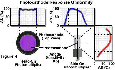
Photocathodes rarely exhibit uniform sensitivity over the entire surface area, and the usual practice in microscopy is to disperse the incident illumination over a substantial portion of the exposed photocathode. End-on photomultipliers usually have larger and more uniform photosensitive regions (see Figure 4), whereas side-on devices exhibit faster rise times and reach a higher level of responsivity due to their opaque photocathodes that do not suffer the optical losses associated with the semi-transparent materials used in end-on devices. In the case of side-on photomultipliers, the upper half of the photocathode is typically 20 to 30-percent more sensitive than the lower half, whereas head-on tubes exhibit a far more uniform response across the entire photosensitive area. Spatial uniformity of the photomultiplier response is another factor determined by the surface uniformity of the photocathode. The collection efficiency of photoelectrons by the dynode chain varies with their emission location on the photocathode and influences the overall spatial uniformity of the photomultiplier. This effect is due to the fact that the stability of the electron multiplication process relies on the electrons following well-defined trajectories.
Photomultipliers used in confocal microscopy are exemplified by the Hamamatsu R3896 side-on design. This unit is equipped with a high quantum efficiency multialkali photocathode having a significant spectral response between 185 and 900 nanometers, and exhibiting a maximum response at 450 nanometers (in the blue-violet region; see the blue curve in Figure 2). The quantum efficiency at 550 nanometers is approximately 22 percent, but drops to only 14 percent at 633 nanometers. The photocathode is illuminated through an ultraviolet glass window material, and has a minimum effective area of 8 × 24 millimeters, while the dynode is a circular-cage design with nine stages. Maximum voltage ratings between the anode and cathode and between the anode and last dynode are 1250 and 250 volts, respectively. These tubes exhibit a typical gain of approximately 10 million with a dark current of about 10 nanoamperes. The anode pulse rise time is 2.2 nanoseconds, while the electron transit time is 22 nanoseconds. Among the many applications for this photomultiplier include flow cytometry, DNA sequencing, fluorescence and Raman spectrometers, ultraviolet-visible spectrophotometers, and particle counters.
Photomultiplier Noise
Detection of the true optical signal distinguished from an unavoidable level of background noise is the primary goal of photometry, quantitative video, and confocal microscopy. The high gain and large signal amplitude capabilities of a photomultiplier are often mistaken as an indicator of superior signal quality. In fact, the internal gain of any detector is only able to amplify the signal presented to the sensor element. If a significant amount of noise is present in the photon-generated signal, the amplified signal will also contain the same noise ratio. High gain detectors benefit from the ability to raise the signal level above the noise floor of the accompanying signal processing electronics. Thus, if the processing electronic circuits limit the signal-to-noise ratio, high gain detectors can dramatically improve signal quality.
The primary sources of noise in any electro-optical system are photon shot noise, detector dark noise, and the amplifier noise arising from accompanying signal processing electronics. Shot noise, due to the quantum mechanical nature of electromagnetic radiation, is inherent in all optical signals and results from stochastic fluctuations in photon arrival times at the sensor. Photons absorbed by or reflected from the surface of a photocathode emit photoelectrons at random intervals to produce a current variation that appears as noise. In the case of low signal levels with high gain photomultipliers, this noise is attributed to background photon flux. The majority of the noise in a photomultiplier arises from statistical variations in the dark noise (referred to with the variable, D), as well as in the shot noise associated with detected photon flux (S). Accurate quantitative analysis requires a photon flux of sufficient magnitude and a sampling time long enough to ensure distinction of the true signal from noise.
As just discussed, statistical variation in the photon flux results in shot noise (N(s)), which equals the square root of the photon signal. Dark noise fluctuations are also randomly distributed, yielding a noise component (N(d)) equal to the square root of the dark current (discussed below). The signal-to-noise ratio (S/N) is therefore equal to the signal divided by the sum of the noise terms added in quadrature:
Photomultipliers produce a signal in the absence of any incident illumination on the photocathode. This effect is termed dark current (or dark noise), and is due primarily to thermal emission of electrons from the photocathode and first few dynodes of the electron multiplier, along with a smaller contribution from leakage current between the dynodes and ground. Secondary sources of dark current are cosmic rays and radioactive decay of materials inside the tube or external high-energy radiation from nearby sources (such a motors, generators, and indoor illumination). Because a single electron, regardless of the source, can induce the release of multiple electrons from each dynode, the photomultiplier chain noise effects are multiplicative. However, the devices are still superior in signal-to-noise level than most electronic amplifiers.
System electronic noise also contributes to dark current and is often included in the specifications for the dark current value. In many cases, photomultipliers are cooled to reduce the levels of dark current and to prevent fluctuations in room temperature from altering device gain or dark current. Cooling the photomultiplier also alters sensitivity, but these changes are smaller than temperature-induced changes in dark current, so a significant improvement in signal-to-noise is observed in cooled devices. Commercial confocal microscopes generally do not employ cooled photomultipliers, however, and are designed to provide satisfactory response at ambient temperatures. When operated in the pulse or photon counting mode, the larger amplitude of the electronic pulse due to photon detection is used to help discriminate photons from dark current.
Practical Confocal Microscope Photomultiplier Operation
In modern commercial confocal microscopes, the photomultiplier is located within the scan head or an external housing, and the gain, offset, and dynode voltage are controlled by the computer software interface to the detector power supply and supporting electronics. The voltage setting is used to regulate the overall sensitivity of the photomultiplier, and can be adjusted independently of the gain and offset values. The latter two controls are utilized to adjust the image intensity values to ensure that the maximum number of gray levels is included in the output signal of the photomultiplier. Offset adds a positive or negative voltage to the output signal, and should be adjusted so that the lowest signals are near the photomultiplier detection threshold. The gain circuit multiplies the output voltage by a constant factor so that the maximum signal values can be stretched to a point just below saturation. In practice, offset should be applied first before adjusting the photomultiplier gain. After the signal has been processed by the analog-to-digital converter, it is stored in a frame buffer and ultimately displayed on the monitor in a series of gray levels ranging from black (no signal) to white (saturation). Photomultipliers with a dynamic range of 10 or 12 bits are capable of displaying 1024 or 4096 gray levels, respectively. Accompanying image files also have the same number of gray levels. However, the photomultipliers used in a majority of the commercial confocal microscopes have a dynamic range limited to 8 bits or 256 gray levels, which in most cases, is adequate for handling the typical number of photons scanned per pixel.
Changes to the photomultiplier gain and offset levels should not be confused with post-acquisition image processing to adjust the levels, brightness, or contrast in the final image. Digital image processing techniques can stretch existing pixel values to fill the black-to-white display range, but cannot create new gray levels. As a result, when a digital image captured with only 200 out of a possible 4096 gray levels is stretched to fill the histogram (from black to white), the resulting processed image appears grainy. In routine operation of the confocal microscope, the primary goal is to fill as many of the gray levels during image acquisition and not during the processing stages.
The offset control is used to adjust the background level to a position near zero volts (black) by adding a positive or negative voltage to the signal. This ensures that dark features in the image are very close to the black level of the host computer monitor. Offset changes the amplitude of the entire voltage signal, but since it is added to or subtracted from the total signal, it does not alter the voltage differential between the high and low voltage amplitudes in the original signal. For example, with a signal ranging from 4 to 18 volts that is modified with an offset setting of -4 volts, the resulting signal spans 0 to 14 volts, but the difference remains 14 volts.
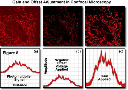
Presented in Figure 5 are a series of diagrammatic schematics of the unprocessed and adjusted output signal from a photomultiplier and the accompanying images captured with a confocal microscope examining mitochondrial fluorescence in living adherent Indian Muntjac deer skin fibroblast cells treated with MitoTracker Red CMXRos. Figure 5(a) illustrates the raw confocal image along with the signal from the photomultiplier. After applying a negative offset voltage to the photomultiplier, the signal and image appear in Figure 5(b). Note that as the signal is shifted to lower intensity values, the image becomes darker (upper frame in Figure 5(b)). When the gain is adjusted to the full intensity range (Figure 5(c)), the image exhibits a significant amount of detail with good contrast and high resolution.
The photomultiplier gain adjustment is utilized to electronically stretch the input signal by multiplying with a constant factor prior to digitization by the analog-to-digital converter. The result is a more complete representation of gray level values between black and white, and an increase in apparent dynamic range. If the gain setting is increased beyond the optimal point, the image becomes "grainy", but this maneuver is sometimes necessary to capture the maximum number of gray levels present in the image. Advanced confocal microscopy software packages ease the burden of gain and offset adjustment by using a pseudo-color display function to associate pixel values with gray levels on the monitor. For example, the saturated pixels (255) can be displayed in yellow or red, while black-level pixels (0) are shown in blue or green, with intermediate gray levels displayed in shades of gray representing their true values. When the photomultiplier output is properly adjusted, just a few red (or yellow) and blue (or green) pixels are present in the image, indicating that the full dynamic range of the photomultiplier is being utilized.
Established techniques in the field of enhanced night vision have been applied with dramatic success to photomultipliers designed for confocal microscopy. Several manufacturers have collaborated to fabricate a head-on photomultiplier containing a specialized prism system that assists in the collection of photons. The prism operates by diverting the incoming photons to a pathway that promotes total internal reflection in the photomultiplier envelope adjacent to the photocathode. This configuration increases the number of potential interactions between the photons and the photocathode, resulting in an increase in quantum efficiency by more than a factor of two in the green spectral region, four in the red region, and even higher in the infrared. Increasing the ratio of photoelectrons generated to the number of incoming photons serves to increase the electrical current from the photomultiplier, and to produce a higher sensitivity for the instrument.
Photomultipliers are the ideal photometric detectors for confocal microscopy due to their speed, sensitivity, high signal-to-noise ratio, and adequate dynamic range. High-end confocal microscope systems have several photomultipliers that enable simultaneous imaging of different fluorophores in multiply labeled specimens. Often, an additional photomultiplier is included for imaging the specimen with transmitted light using differential interference or phase contrast techniques. In general, confocal microscopes contain three photomultipliers for the fluorescence color channels (red, green, and blue; each with a separate pinhole aperture) utilized to discriminate between fluorophores, along with a fourth for transmitted or reflected light imaging. Signals from each channel can be collected simultaneously and the images merged into a single profile that represents the "real" colors of the stained specimen. If the specimen is also imaged with a brightfield contrast-enhancing technique (such as differential interference contrast), the fluorophore distribution can be overlaid to determine the spatial location of fluorescence emission within the structural domains.
Analog Signal Detection versus Photon Counting
Photomultipliers, due to their low noise level and high bandwidth, prove to be excellent, almost distortion-free detectors when the optical signal is of short duration and very weak (such is often the case in confocal microscopy). They can be operated in either analog or digital mode, depending upon the level of incident illumination. At bandwidths below 100 megahertz, the signal can be detected as a series of pulses on the anode and processed digitally. Above this level, the interval between light pulses becomes so short that they overlap to produce a continuous waveform, and it becomes necessary to employ analog signal processing electronics to adequately sample the output. Sampling of anode pulses at low light levels is usually accomplished with an integrate-and-hold circuit, whereas when the photomultiplier operates in analog mode, a transresistance amplifier is used to measure tube current.
In many confocal microscopy applications, the specimen is fixed and sufficiently labeled with a fluorescent probe having a high quantum yield at the laser excitation wavelengths. During a typical pixel dwell time of 1-2 microseconds, between 200 and 1000 secondary emission photons will successfully pass through the microscope optical system and impact on the photomultiplier sensor. However, some specimens contain only a minute amount of fluorophore and emit small quantities of photons, sometimes at levels below 10-20 photons per pixel for stained features, and either zero or only a couple of photons in the unstained regions (the latter often constitutes the majority of the pixels in a scan). In this case, photon counting becomes the preferred mechanism of detector operation.
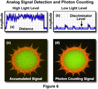
The graph in Figure 6(a) illustrates typical photomultiplier pulse output at high light levels, which can be easily sampled as an analog signal using a conventional analog-to-digital converter. In contrast, the more discrete nature of pulse generation by the photomultiplier when operated at the very low light levels experienced with poorly stained specimens is presented in Figure 6(b). By integrating or accumulating this signal as it is received from the detector, the low level noise associated with the signal reduces image contrast and increases the background intensity (Figure 6(c)). However, when a discriminator is used to set the intensity level necessary for signals to be processed by the converter (Figure 6(b), red line), the image contrast is dramatically increased and background noise is sharply reduced (Figure 6(d)). Sophisticated photon counting techniques conducted with the proper instrumentation result in a linear response with an increase in signal-to-noise when compared to analog detection.
The gain from each stage in the dynode chain is subject to multiplicative noise due to the Poisson statistics of photoelectrons emitted by the photocathode. In a typical photomultiplier, the number of electrons arriving at the second dynode as a result of a single collision at the first dynode can range between 2 and 20. As an example, if the average number of electrons emitted by the first dynode is 9, then according to Poisson statistics, the number arriving at the second dynode will range between 6 and 12. A photoelectron that sends 12 electrons to the second dynode obviously has the potential to generate a substantially larger pulse than one that sends only 6 electrons.
Although this effect occurs at every dynode in the multiplier chain, the implications are most important between the first and second dynodes because of the relatively low number of quantum events in these stages. As a result, the variation in single photocathode pulses from the photomultiplier can range over an order of magnitude, although they tend to cluster around a mean value. Multiplicative noise in photomultipliers tends to stretch the number of gray levels (between 0 and 255) recorded by the analog-to-digital converter, resulting in histograms that feature pixels at almost every gray level, regardless of the fact that they may have arisen from only a few initial electrons at the first dynode. In other words, the phenomenon of multiplicative noise presents the illusion of a full gamut of gray levels on the host computer monitor when the data accumulated by the microscope are limited to only 3 or 4 clearly defined gray levels.
As discussed above, the Poisson statistical signal-to-noise ratio is equal to the square root of the number of detected photons in confocal and other forms of optical microscopy. Therefore, a signal of 100 photons per pixel results in a noise level of approximately 10 photons, or 10-percent of the total signal. In most cases, the detected signal is directly fed into an 8-bit analog-to-digital converter, which has a digital resolution of approximately 0.4-percent per gray level (256 gray levels). Because the converter is capable of detecting more than 65,000 photons per pixel at this resolution, it is easily capable of reproducing a suitable image from a typical fluorescent specimen at the fluctuating signal levels experienced with confocal microscopy.
Troubleshooting Photomultipliers
Because of they are designed to operate at relatively low light levels and are delicate vacuum tubes containing optical windows, photomultipliers should be handled with extreme caution and care. The outer glass surface should remain free of fingerprints, dust, debris, and oils (don't touch a photomultiplier without protective gloves). The photocathode element is extremely light sensitive, so room lighting should be reduced before manipulating the tubes. One of the most obvious problems encountered with photomultipliers is the onset of current pulses at lower voltages, resulting in rapid changes in gain (up to 20 percent variation in a few seconds). In most cases, the origin of this problem is leakage of atmospheric gases into the vacuum tube. A leaking photomultiplier tube can often perform satisfactorily at lower voltages for some time, but they cannot be re-sealed and must ultimately be replaced. High levels of dark current, manifested by an excessive amount of signal in the absence of incident illumination on the photocathode, is another symptom of photomultiplier failure that usually occurs after exposure of the tube to excessive light levels. The situation is compounded if the photomultiplier has a high voltage applied to the dynode chain when the exposure occurs. As in the case of leaking tubes, the photomultiplier cannot be repaired and must be replaced.
Unstable signal levels in confocal microscopy are often the result of problems not associated with the photomultiplier. Specimen photobleaching, a gradual reduction of fluorescence intensity over a period of time, should not be confused with instrument malfunction. Laser power supplies (especially helium-neon versions) can experience fluctuations in output, intermittent noise, or complete failure that at first may appear to be a problem with the photomultiplier. If signal levels are unstable and the laser power supplies, photomultiplier high-voltage supply, and amplifiers are operating satisfactorily, there may be a light leak in the instrument. The photomultiplier pins and socket connections should be periodically checked by a qualified technician, and cleaned or tightened to avoid an buildup of oxide that can produce short circuits and hamper performance.
Conclusions
Electronic imaging sensor performance, including that of photomultipliers, is described by the spectral sensitivity, quantum efficiency, spatial resolution, uniformity, signal-to-noise ratio, dynamic range, and response speed (some of these variables are listed in Table 1). The spectral sensitivity is an important term that determines the level of signal as a function of the wavelength of incident light. It is often expressed in terms of the quantum efficiency, which is a percentage of incident photons that are detected. The uniformity of photomultipliers and other electronic detectors is determined by several variables, including gain variations across the sensor, along with regional differences in noise and the efficiency of sampling (often termed shading with imaging detectors and non-uniform sensitivity with photomultipliers). Spatial variation in the efficiency of light collection or transmission also affects the uniformity of detector response.
The limiting spatial resolution is usually determined from the minimum separation distance required for discrimination between two high-contrast specimen features (for example, white points or lines on a black background). Contrast is an important factor in resolution because high contrast features are more easily resolved than low contrast features. More informative measures of the spatial resolution of an electronic detector are the modulation transfer function (MTF) and the contrast transfer function (CTF). Both functions display the magnitude of the detector response as a function of spatial frequency. The contrast function is determined from the detector response to a series of black and white bars that become narrower and closer together, while the modulation function is similarly determined from the image of 60-percent contrast sine waves of increasing spatial frequency.
Performance Characteristics
of Popular Detectors at 550 Nanometers
| Detector | Quantum Efficiency (Percent) | Sensor Noise (Electrons/Pixel) | Detector Gain |
|---|---|---|---|
| R3896 Photomultiplier | 20 | 0 | 9,500,000 |
| Avalanche Photodiode | 75 | 5-20 | 50-200 |
| Silicon PIN Photodiode | 80-85 | 100 | 0 |
| Cooled Interline CCD | 40-60 | 8-12 | 4 |
| Intensified MCP CCD | 30-45 | 100 | 10,000 |
| Electron Bombardment CCD | 30 | 40 | 100-300 |
| Vidicon Video Tube | 50-60 | 1000-2000 | 8-10 |
Table 1
Electronic detectors are often compared by their signal-to-noise ratio, a measure of the variation of a signal that indicates the confidence with which the magnitude of the signal can be estimated. Light has an inherent noise component arising from the stochastic nature of the photon flux (and governed by Poisson statistics), which is equal to the square root of the signal. Noise also derives from a variety of other sources, but can often be reduced by lowering the operating temperature. The thermally sensitive noise present in electronic devices in the absence of light is termed dark noise. Photomultiplier gain levels range from 1000 to 10 million, and the anode output is usually fed directly into an electronic amplifier. To avoid having the system noise dominated by the amplifier, the photomultiplier should be operated at gain levels high enough so that the product of the dark current and the gain is larger than the amplifier input noise.
Intrascene dynamic range is derived from the maximum and minimum intensities that can be simultaneously detected in the same field of view. Interscene dynamic range is the range of intensities that can be accommodated when the detector gain, integration time, lens aperture, and other variables are adjusted for differing fields of view. Dynamic range and signal-to-noise ratios should not be confused. Dynamic range is often calculated to be the maximum signal that can be accumulated, divided by the noise associated with reading the signal.
In laser scanning confocal microscopy, the specimen is scanned in a raster pattern by the focused illumination beam, and the resulting fluorescence emission forms a point image that is sequentially detected by a photomultiplier. Most commercial confocal microscopes feature photomultipliers that are limited in dynamic range to 8 bits or 256 gray levels with a wavelength-dependent detection efficiency ranging between 15 and 30 percent. Compared to cooled CCD cameras, which typically feature 10 to 12-bit dynamic range and 40-60 percent detection efficiency over a wide wavelength range, photomultiplier performance is significantly less. However, in a majority of confocal applications (especially live-cell imaging) fewer than 255 photons per pixel are collected, well within the dynamic range of the photomultiplier tube. Furthermore, the excellent linearity of the photomultiplier response and background noise rejection properties render this detector ideal for confocal microscope applications.
Confocal microscopes, spectrophotometers, and many high-end automatic camera exposure monitors utilize photomultipliers to gauge and record light intensity. Unfortunately, the most serious light losses in confocal microscopy occur with the limited quantum efficiency of the photomultiplier. Spectral sensitivity of the photomultiplier depends on the chemical composition of the photocathode with the best devices having gallium-arsenide-phosphide elements (with a quantum efficiency of about 40 percent in the green spectral region), which are sensitive over a wavelength range from 300 to 800 nanometers. Photomultiplier photocathodes are not uniformly sensitive and typically the photons are spread over the entire entrance window rather than in one region. Because photomultipliers do not store charge and respond to changes in input light fluxes within a few nanoseconds, they can be used for the detection and recording of extremely fast events. Finally, the signal to noise ratio is very high in scientific grade photomultipliers because the dark current is extremely low (it can be further reduced by cooling) and the gain may be greater than one million.