Next-Generation SilVIR Detector System for the FLUOVIEW FV4000 Laser Confocal Microscope
Abstract
Evident has pioneered the proprietary, next-generation SilVIR detector system for the FV4000 laser confocal microscope. This detector sets a new benchmark in multicolor imaging, offering exceptionally low noise and high sensitivity with an impressive signal-to-noise (S/N) ratio across the visible to near-infrared wavelength range. With its ability to accurately detect photons, including high-speed and high dynamic range photon counting, the SilVIR detector helps ensure experimental
repeatability. Moreover, it introduces a streamlined operational experience by eliminating the need for gain adjustments commonly required with PMT detectors. Its excellent performance sets the SilVIR detector on a trajectory to become the industry's new standard for laser scanning microscopy.
1. Introduction
Photomultiplier tubes (PMTs), which can detect weak light at several photon levels with high sensitivity and high gain, have been the standard detectors for laser scanning microscopy (LSM) to capture very weak fluorescent light. Nonetheless, there are a number of issues associated with LSMs utilizing PMTs, which will be discussed in the following sections.
The SilVIR detector system uses a semiconductor-type sensor to detect fluorescence. This silicon photomultiplier (SiPM) eliminates many of the issues and restrictions of conventional PMTs. The signal processing circuit also incorporates technology that maximizes the sensor’s capabilities, expanding its applicability to high-pixel-number and high-speed imaging (Figure 1).
In this article, we describe the problems surrounding conventional LSM imaging using PMT detectors and describe how the SilVIR detector can solve them.
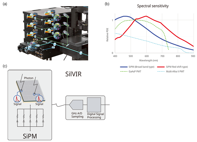
Figure 1. The devices that comprise the SilVIR detector: (a) the FV4000 fluorescence detector; (b) a graph showing the the SilVIR detector’s spectral sensitivity—the detector has a higher sensitivity than conventional high sensitivity GaAsP-PMTs from 400 nm to 900 nm using a broadband type and red-shifted type; (c) the SilVIR detector is comprised of a SiPM sensor, 1 GHz A/D sampling, and digital signal processing.
2. The Needs of Laser Scanning Microscopists—Building a Better Detector
Common complaints of LSM users include:
- Confusion over which settings to adjust to maximize device performance.
- Too much photobleaching and phototoxicity.
- Unintentional saturation of the detectors.
- The need for better image quality, resolution, and frame rate.
- An inability to acquire better images.
The root of these complaints is the PMT detector and its principal method of operation. Below, we discuss some of the factors we considered when setting out to build a better detector.
High sensitivity and signal-to-noise (S/N) ratio
To efficiently detect even a small amount of incident photons—as is required for imaging with weak fluorescent signals—it is essential that the detector have a high quantum efficiency (QE) and photodetection efficiency (PDE). In addition, the intrinsic noise of the sensor and detector circuitry must be negligible to achieve a high S/N ratio.
Quantification of detected light
Although there are various definitions of the physical measurement of detected light, the quantification of "photon number" is the most accurate way to quantify very weak fluorescence light. Therefore, the simplest way of measuring intensity is the number of detected photons (Figure 2).
Quantifying fluorescence intensity using a numerical value is very important. For example, this makes it possible to reproduce the same imaging results on different instruments because it is not a device-specific value. Furthermore, because the photon number value is universal, researchers can more easily share data with each other. Lastly, the quantitative values can be used as an indicator for pre-processing images during analysis.
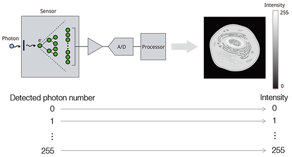
Figure 2. The fluorescence detection process starts when photons are incident on the photo-sensor’s surface. The detected photons are then converted to electrons and amplified and output as an electric current. The current is analog-digital converted after passing through the amplification circuit. Then, the digitalized signal is converted to an intensity value for each pixel by arithmetic processing and is visualized as each pixel in the image by the software.
High dynamic range
Even if the above items can be realized, if the maximum number of photons detectable at a given time—known as dynamic range—is small, intensity saturation will occur in the regions where the fluorescence intensity is high, and the quantitativity will be lost. Furthermore, one of the ways to improve image quality is to suppress photon noise (the probabilistic noise of photon detection at the sensor, also known as shot noise) by increasing emission photons with strong excitation. High-quality images can be captured without saturating the brightness when dynamic range is high. For example, as shown in Figure 3, the more fluorescent light that is detected by the stronger excitation on the right, the better the image quality. However, ultimately, the saturation of the detectors will jeopardize many post-processing and analysis steps.
Consistent detector gain for image quantification
It is ideal to have high dynamic range without changing the conditions of the detector or circuit. For example, if the detector gain is changed to extend the upper range, the resulting intensity of the image also changes. However, this relationship is not linear, making it difficult to inversely estimate the detected light amount only from the obtained image. A calibration curve must be prepared separately for correction. On the other hand, the line chart plots in Figure 3 show the brightness profile across line A on each image. When these are obtained with a fixed detector setting, the detected numbers of photons at each pixel can be quantitatively estimated from the intensity of any image.
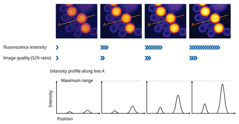
Figure 3. The relationship between fluorescence intensity and image quality. The signal-to-noise ratio is determined by the fluorescence intensity/√fluorescence intensity.
3. Conventional PMT Detector Issues in LSM Imaging
Below, we discuss the primary issues when using a PMT detector for laser scanning microscopy.
It is difficult to achieve both high sensitivity and a high S/N ratio
Currently, it is common to use GaAsP photocathode-type PMTs [1], whose QE in the visible range has been improved to 40% or more, as a high-sensitivity detector. Because of the noise from the sensors and circuits, it has been generally used by amplifying the signal with a higher gain to prevent the relative noise from affecting the image. A PMT also converts photons into electrons at the light-receiving surface, which then undergo a stochastic, multistep amplifying process to generate a current signal (Figure 4). Therefore, even if the number of detected photons is constant, the output changes each time due to stochastic fluctuation. This may reduce the image S/N ratio, particularly for high-pixel, high-speed imaging with fewer detected photons.
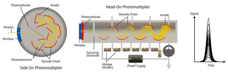
Figure 4. The structure of a PMT’s input-output characteristics. When photons are incident on the photocathode, emitted electrons from the photocathode are amplified in a vacuum tube. As secondary electrons are repeatedly amplified at multiple dynode chains, the output pulse signal when detecting one photon is not uniform or stable.
Low quantitativity of intensity for detected photons
As described above, a PMT has a stochastic variation during photoelectron amplification. Therefore, the input/output quantitativity is low, particularly when the photon-detection rate is low. In addition, while the gain can be adjusted by varying the voltage applied between the electrodes, the corresponding ratio of input and output also changes. Even if the same voltage is applied, the actual gain varies greatly between each PMT because of individual differences. And when the applied voltage is set at a low level to amplify large amounts of photons, it worsens the linearity.[1]
Furthermore, the following unavoidable phenomena will cause the PMT’s sensitivity to deteriorate according to the accumulated detected photons by usage.
- When photons enter the photocathode, electrons are emitted from the photocathode into the vacuum tube due to the external photoelectric effect. The photocathode deteriorates because electrons cannot be fully replenished.
- Degradation of dynodes due to collision with electrons (photoelectrons) emitted from the photocathode.
- Deterioration of the photocathode or dynodes due to collision with ions generated by the collision of photoelectrons with residual gas or impurities in the vacuum tube.
- Decrease in vacuum due to impurities generated from dynodes due to the collision of photoelectrons with dynodes.
Because of the above, LSMs using PMTs cannot provide quantitativity between the detected light amount and the image intensity.
It is difficult to achieve both high dynamic range and high S/N ratio
When the sensor gain is increased, a weak signal of a few photons can still be detected despite the noise, enabling a high S/N ratio to be achieved. But the upper limit of the PMT's output current is as low as several μA. If the gain is set high, the output will be easily saturated, even by the small number of detection photons, resulting in a small dynamic range (Figure 5a). On the other hand, if the gain is low, the output signal will not be saturated even when strong fluorescence (a large number of photons) is detected, and the dynamic range will be higher. However, weak fluorescence, such as several photons, will not be amplified and will be buried in the noise, causing the S/N ratio to deteriorate (Figure 5b). The result is that the user needs to manually adjust the detector's gain in accordance with the brightness of the object and the required image quality level. In addition, there is a disadvantage that the dynamic range and S/N ratio are unintentionally changed due to this adjustment.
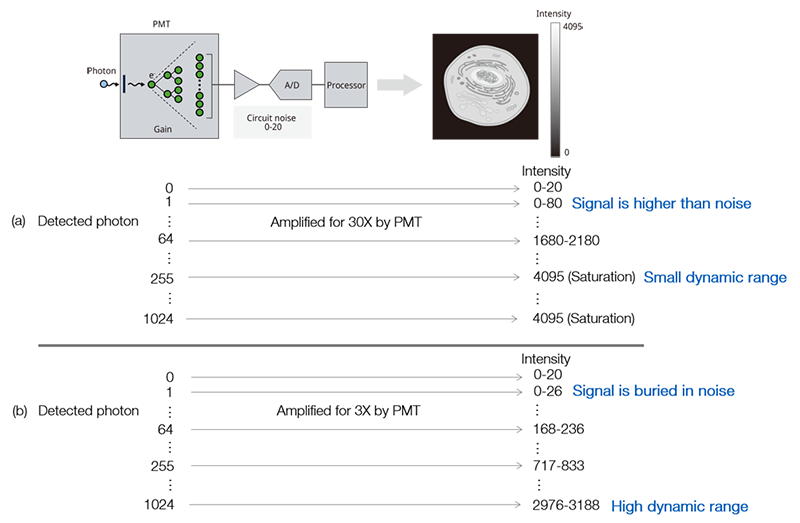
Figure 5. Adjusting a PMT’s gain requires balancing the signal-to-noise ratio and the dynamic range; (a) high gain—the ouput signal can be amplified higher than the noise when detecting one photon but it reduces the dynamic range, and it is easy to get saturated; (b) low gain-the output signal cannot be distinguished from the noise when detecting a few photons. On the other hand, the dynamic range is higher, and it does not get saturated when detecting a large number of photons.
Complex detection settings
Adjusting the detector settings to obtain satisfactory image quality while avoiding brightness saturation is complicated, making it difficult for users who are not skilled in LSM. For explanatory purposes, Figure 6 shows fluorescent beads with different fluorescence intensities caused by different detector gain settings.
Figure 6a shows the beads under different excitations acquired with high gain. Dark beads can barely be distinguished from the noise, even by weak excitation (the leftmost image of the figure), but the bright beads became saturated when the excitation light increased (the two bright bead portions on the right side of the figure).
On the other hand, Figure 6b shows the same fluorescent bead images acquired using a lower gain. The signal of the dark beads under weak excitation (the two on the left side of the diagram) was buried in the noise. It is superior to high gain in that the bright beads did not saturate even when the excitation was set to the highest level (rightmost side in the diagram), but it did not have a better S/N ratio than the rightmost image of Figure 6a (image captured using high gain) when focusing on the S/N ratio of the dark beads.
Typical fluorescent images of cell specimens have significant brightness differences by region, and time-lapse or Z-stack images can have even greater differences in brightness throughout the stack. It is difficult for even experienced users to find the optimum detector settings to obtain images with a satisfactory S/N ratio in dark areas without saturating the bright areas. Many users make trial-and-error adjustments of detector gain, excitation light intensity, exposure duration, etc., and this can lead to microscopists acquiring many failed images.
When the S/N ratio is insufficient due to detector settings that do not cause saturation, the S/N ratio can be improved by capturing multiple frames and averaging or accumulating them to suppress only random noise. In this case, many frames need to be captured, and it results in a significant drop in the actual imaging frame rate.
As described above, adjusting complicated imaging parameters, such as detector gain, excitation light intensity, and exposure duration, as well as the number of averaging times between frames are required for conventional LSM using PMTs.
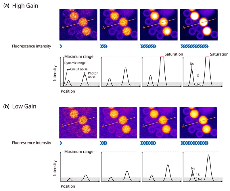
Figure 6. Adjusting a PMT’s gain requires balancing the signal-to-noise ratio and dynamic range, which can be difficult. The images were acquired using different excitation laser settings, with the images on the right being acquired using a higher setting. The plots below the images show the intensity profile along line A. The signal-to-noise ratio is the ratio of S (the profile height) and Ns (photon noise) and Nd (circuit noise). Figure 6a shows samples acquired using high gain. The dim beads have a higher S/N ratio, but the brighter beads get saturated. Figure 6b shows samples acquired using low gain. The dim beads have a lower S/N ratio, but the bright beads do not get saturated.
Detection circuit issues
There are also issues in the detection circuit as well as sensors. Since the sensor signal and its amplifying circuitry are noisy, the S/N ratio becomes very low when the raw signal sampled by analog-to-digital (AD) converters is processed as pixel data (Figure 7a, left). In general, this S/N ratio can be improved to be equivalent to the true value of the fluorescent intensity by sampling the signal after smoothing with a low-pass filter or integrator in the analog detection circuit (Figure 7a, right). However, the faster the scan speed, like a resonant scanner, the shorter the time it takes to traverse the structure of the specimen. Figure 7b shows the fluorescent image of the same structure as shown in Figure 7a except that it is scanned at twice the speed compared to Figure 7a. If a low-pass filter for noise reduction is applied in the same way, the time resolution to resolve the fine structures with high spatial frequency will be insufficient, and the spatial resolution of the resulting image will be degraded (Figure 7b, right).
When the cutoff frequency of the low-pass filters is increased, the time-resolution improves. However, the noise-suppression effectiveness is degraded, and the S/N ratio deteriorates. To avoid a decrease in the S/N ratio, even if the cutoff frequency of the low-pass filters is increased, it is necessary to increase the AD converters’ sampling rate from several times to several tens of times the pixel clock to perform a large number of samplings within one pixel (oversampling). In addition, the faster scanning speed and higher pixel number shorten the dwell time of one pixel, which is why the faster sampling speed of the AD converters is required.
For noise smoothing, another problem is that the analog circuit can only adopt a simple filter—such as a low-pass filter—at the expense of time resolution. A filter method that separates only noise without sacrificing time resolution by applying advanced digital signal processing filters on data sampled at high speed is desirable.
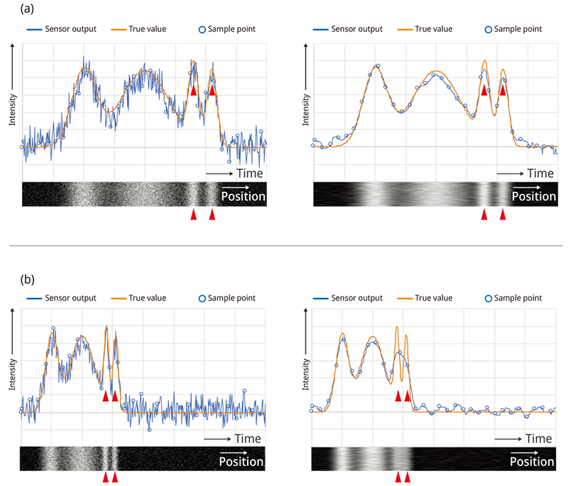
Figure 7. The effect of reducing the noise on the image quality and spatial resolution. Figure 7a was captured at standard scan speed, and the image quality was improved by reducing the noise. Figure 7b was captured at a scan speed two times faster than what was used in 7(a), and you can see that the spatial resolution is degraded because of the signal bandwidth drop.
The above LSM imaging issues caused by PMTs can be solved using our SilVIR detector, which combines a new semiconductor-type SiPM sensor with high-speed digital sampling. In the next section, we'll explain how we've solved the issues above using our advanced technologies.
4. SilVIR Detector Technical Introduction
4-1. SiPM Features
The SiPM sensor at the core of the SilVIR detector is a semiconductor sensor comprised of a two-dimensional array of thousands of Geiger-mode avalanche photodiodes (APDs; single-photon counting avalanche photodiode, or SPAD). The detected signals are output as the sum of all APDs [2] (Figure 8).
Geiger mode allows one-photon incidence to be detected at high signal levels by a highly stable multiplication process despite high gain. Furthermore, the semiconductor manufacturing process allows for precise control over the individual variations of SiPMs. Through consistent mass production, the differences in photodetection efficiency (PDE) and gain between SiPMs can be minimized to a high degree. In addition, even if many photons are incident at the same time, the sum of the respective APD currents is output from the SiPM, so the upper limit of the output current is high, resulting in a wide dynamic range to detect a large number of incident photons. In other words, one photon signal can be multiplied with high gain and has a wide detection range. This makes it possible to achieve a high signal-to-noise ratio and a wide dynamic range simultaneously, eliminating the need to compromise between the two by adjusting the gain.
In addition, photoelectric conversion by a SiPM, like photodiodes, uses the internal photoelectric effect where electrons are excited from the valence band to the conductor. Therefore, electrons are replenished quickly when they are excited. The result is that the sensitivity and gain are not degraded, even if there is a large amount of incident light.
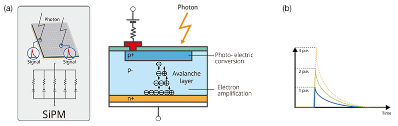
Figure 8. The structure of a silicon photomultiplier (SiPM) sensor and its input-output characteristics. Figure 8(a) shows that a SiPM is comprised of multipixel APDs. When one photon is incident on the APD’s photon receiving surface, the current signal is output by the internal photoelectric conversion followed by avalanche electron amplification at the avalanche layer. Figure 8(b) shows that when multiple photons are incident simultaneously, the output signal is the sum of the APD signal. The output waveform of the APD in response to the detected photon is constant and stable.
In addition, the SiPM sensor has excellent sensitivity characteristics. Figure 1b shows the spectral sensitivity of the SiPM sensor. Using a combination of SiPM sensors with different spectral sensitivities—which we call the broadband silicon detector (BSD) and red-shifted silicon detector (RSD)—you can achieve better sensitivity than a GaAsP-PMT detector in the visible (400 nm) to the near-infrared (900 nm) wavelength range. The photon detection efficiency (PDE) of the SiPM is defined by the equation:
PDE = QE × FF × AP
QE: Quantum efficiency
FF: Aperture efficiency (fill factor)
AP: Probability of Geiger mode (avalanche probability)
The FF is determined by the area of the APD on the SiPM photon receiving surface relative to the area of the dead zone between APD pixels. AP is dependent on the voltage applied to the SiPM—the higher the voltage, the higher the PDE that can be achieved. On the other hand, increasing the applied voltage will increase the noise of the sensor. For example, in the S13360-3050 model made by Hamamatsu Photonics, the PDE can be increased by about 1.4 times by increasing the overvoltage (voltage applied above the breakdown voltage) from 3 V to 7 V, but the dark count noise is increased by about 2 times, the crosstalk noise by more than 2 times, and the after pulse noise by more than 3 times [2]. This increased noise will offset the benefits of the increased PDE and, consequently, will not improve the S/N ratio. In addition, the increased noise greatly hinders the quantitativeness of photon detection, which is one of the major benefits of SiPMs. Furthermore, since the gain is also increased by a factor of two or more, the detection dynamic range becomes smaller. An illustrative example of the potential pitfalls of solely focusing on high PDE or QE values serves as a reminder to avoid blindly pursuing such characteristics, as they may result in unintended drawbacks. For this reason, the FV4000 confocal microscope uses a SiPM with optimum overvoltage to obtain balanced noise level and sensitivity and an outstanding dynamic range for fluorescence detection.
The fact that a SiPM has a higher dark count noise than a PMT is often cited as a disadvantage. As a countermeasure, the photon receiving surface is cooled to approximately -20 °C (-4 °F) to reduce the dark count noise to between several kilocounts to several tens of kilocounts per second. But this is still larger than the cooled PMT. However, when a SiPM with a dark count noise of 10 kilocounts per second is used for scanning at 512 pixels/line at 2 µs/pixel dwell time, a dark count noise equivalent to 1 photon appears in only about 10 pixels per 1 line. At this amount, there is little impact on LSM image quality.
Another disadvantage of using a SiPM as a LSM detector is that a long tail decay may remain in the output signal (Figure 8). This causes an issue in high-speed imaging, but as described in the next section, we have successfully addressed this issue with the implementation of an innovative detection circuitry solution.
4-2. High-speed sampling and digital processing features
As described above, conventional systems balanced the S/N ratio and temporal resolution by combining signal smoothing using analog circuit filtering with the minimum necessary AD sampling frequency (a sampling period of about 1/2 the pixel period) for pixel resolution. However, this solution was technically limited to respond to the higher pixel number (shorter pixel period) by the high-speed resonant scanner (Figure 9a).
High-speed AD sampling
We realized a 1 GHz AD sampling rate, which is 12 times faster than the conventional sampling rate, and adopted an oversampling method in which a large amount of sampling is performed within one pixel period. Since a SiPM sensor output has a wide dynamic range, the range of its output signal is also very large compared to a PMT. Along with the higher AD sampling rate, the amplitude-resolving accuracy is 16 times higher (from 10-bit to 14-bit) than conventional devices. These high-performance devices are optimized for SiPM signal processing applications. Noise isolation uses a digital-signal-processing filter instead of an analog-circuit filter, which efficiently attenuates noise while minimizing the sacrifice of the signal bandwidth to achieve a higher S/N ratio. As a result, high-frequency components that could not be separated by the conventional method can be detected separately, and sufficient pixel resolution (temporal resolution) can be achieved, even if the pixel number of the resonant scanner is 1k or larger (Figure 9b).
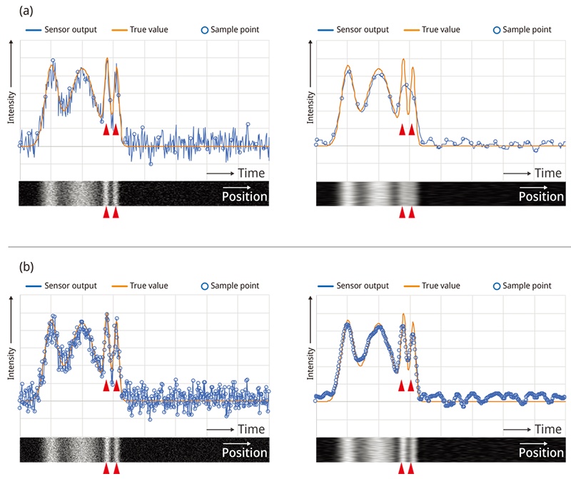
Figure 9. The effect of improved noise reduction on image quality and spatial resolution. Figure 9(a) shows the conventional method with an analog circuit filter and slow speed sampling; the spatial resolution is degraded because of the signal bandwidth drop when the scan is fast. Figure 9(b) shows a combination of high-speed sampling and digital-filter-enabled noise reduction during a high-speed scan while maintaining the spatial resolution.
Real-time inverse transformation at the field programmable gate array to eliminate signal decay
In addition, we have developed a technique for restoring the bandwidth degradation due to slow signal decay, which is a disadvantage of SiPM sensors, by utilizing advanced signal processing at the field programmable gate array (FPGA) with no restrictions. As a technique for eliminating decay signal, there is a known force resetting method [3]. However, our technique can restore the output signal at higher speed without the complicated detection circuitry required by the conventional technique.
While a SiPM sensor can output the photon detection timing and the number of photons detected accurately and quickly, it has one disadvantage—a slowly decaying output signal. When imaging using a resonant scanner, the short pixel dwell time causes the leakage of a decay signal into adjacent pixels, which degrades the pixel resolution and temporal resolution (Figure 10a).
Using a SiPM, the total signal output is the sum of the signal outputs from each APD, and the output response pulse waveform created in response to the photon incidence of each APD is very stable and maintains a constant shape compared to a PMT. If the response to the input can be uniquely defined, the final output can be obtained by the convolution sum of the response to the input. Assuming that the photon detection timing and its number are x(t) at Figure 10b and the sensor response are h(t), the output y(t) is;
y(t)=(x*h)(t)=∑x(i)h(t-i)
When the SiPM output signal y(t), including the decay signal, is measured, if the sensor response h(t) can be defined, the photon detection event x(t) containing no decay signal can be calculated by executing this inverse transformation. This is based on the same concept as a deconvolution filter [4], which is often applied to eliminate the tail of the signal waveform, for example when analyzing spark signals of calcium ion dynamics quantitatively in the neuroscience field. The FPGA features a high-speed, advanced digital-signal processor (DSP) that enables real-time processing of inverse transformation calculations within the device. In fact, we have developed a technique to obtain the output data of the sensor-signal inversely transformed at the FPGA in real time [5], as shown in Figure 10c.
By calculating pixel intensity using this inversely transformed data sequence, we eliminated the leakage of the decay signal into neighboring pixels, as shown in Figure 10a. In addition, the restoration filters not only remove the decay signal but also isolate mixed noises, which differ from the original photon-detection response. This further improves the S/N ratio of the signal.
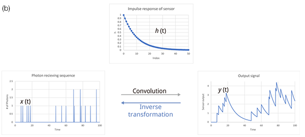
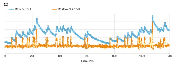
Figure 10. An overview of the technique to restore bandwidth degradation due to the decay signal from the SiPM. Figure 10(a) shows the sensor decay signal and degradation of the spatial resolution; 10(b) shows the relationship input and output of the SiPM sensor; and 10(c) shows the estimation of the input signal by deconvolution.
As shown in Figure 11, if there is no inverse transformation, the image pixel resolution is degraded by the effect of the SiPM signal decay, particularly during high-speed and high-resolution resonant scanning. On the other hand, applying the inverse transformation restores the temporal resolution without losing the photon input, making it possible to obtain a high-resolution resonant scanner image (1024 pixels/line) without the loss of special resolution and or detected photons.
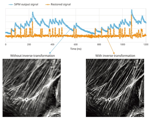
Figure 11. An example showing a sample captured with and without inverse transformation (Actin (BODIPY FL) in a BPAE cell; resonant, average 64, ex. 488 nm, Em. 500–540 nm, same excitation power; UPLSAPO40x2/NA 0.95, CA 1 AU, 1024 × 1024 pixels.
High dynamic range photon counting
Raw SiPM output signals are more prone to be piled up when high-frequency photon-detection events occur, such as the detection of more photons prior to the decay of the signal (the blue line in Figure 11). Therefore, to take advantage of a SiPM’s high dynamic range, the AD converter's conversion scale needs to be larger than the signal amplitude of high-frequency photon detection, including the pile-up effect. On the other hand, to perform the inverse transformation process accurately, the signal amplitude of one photon, which is the smallest signal, must be detected with a fine resolution pitch. Thus, an AD converter with higher resolution is required to capture smaller amplitudes with finer resolution and larger pile-up amplitudes. In addition, inverse transformation is not possible without very high time resolution, i.e., many digital data sequences acquired at fast sampling rates. Generally, AD converters with a 1 GHz sample rate for high-speed devices have an 8-bit degree of resolution. However, we achieved this inverse transformation process by using high-end AD converters with a 1 GHz sample-rate, 14-bit resolution (16384 gradation), and high-speed processing of the large-capacity, high-speed digital data obtained from these converters using a high-end FPGA.
The inversely transformed signal (the orange line of Figure 11) is restored, maintaining the time resolution by removing the decay signal. By leveling the piled up signals, the pulse-output amplitude (wave peak value) corresponding to the detected number of photons can be obtained. In other words, when one photon is detected, pulses with the same amplitude are output. Similarly, when two photons are simultaneously detected, pulses with an amplitude twice as high are output. If photons are simultaneously detected thereafter, the pulses are output with an amplitude that is an integer multiple of that one photon. Therefore, if N photons are detected within a certain time interval, the time integration of these output pulses can be obtained as the integrated intensity of N times the pulse at the time of one photon detection. This relationship also holds true when a large number of photons are detected within a very short time.
Consequently, this method enables the accurate detection of fluorescent light, even when a large number of photons are detected in a short period of time, with a S/N ratio that is capable of detecting photons discretely. As a practical measure, up to 1 gigaphoton per second can be detected with this S/N ratio without saturation. While the conventional single-photon counting (paralyzed or non-paralyzed) [1] could only be applied at low-frequency photon detection rates, the present technique achieves HDR photon counting, which is comparable in S/N to the single-photon counting, even when imaging very bright samples at high speed (Figure 12).
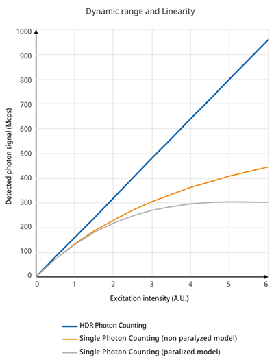
Figure 12. The relationship between excitation intensity and the output signal. The larger number of photons per a certain time can be detected when increasing the excitation power. The output signal gets saturated at a low detected photon rate using a conventional photon counting method. HDR photon counting by the SilVIR detector does not get saturated, even at a high frequency incident photon rate. The graph curves of single photon counting were calculated with 1.2nsec pulse pair resolution.
4-3. SilVIR Detector Advantages
The SilVIR detector system is a combination of a SiPM sensor and high-speed sampled digital processing. In the previous section, we described ideal LSM fluorescence detection and the status of conventional LSM and how it deviates from the ideal. However, we realized near-ideal LSM fluorescence detection using the SilVIR detector.
High sensitivity and S/N ratio
An ideal detection system should have a high photon detection efficiency (PDE) and no sensor or electric circuit noise.
Using two types of SiPM sensors, the SilVIR detector achieves a higher PDE both in the visible range and NIR with no trade-offs between the dynamic range and S/N ratio. In addition, photon shot noise is dominant in the SilVIR detector because electric circuitry noise is suppressed to one photon level or less, and the dark current is negligibly small. Thus, the approximate S/N ratio can be estimated from the number of detected photons by the following equation:
S/N ratio = N/√N = √N
N: number of detected photons
Since the S/N ratio can be more easily quantified, the number of detected photons can be a useful indicator for sharing and discussing images and for reproducing the quality of images in a day-to-day imaging experiment.
Quantitativeness of detected fluorescence intensity
An ideal detector can relate the amount of detected fluorescence and the intensity on a quantitative scale. However, using conventional technology, this relationship was unclear and uncertain. The SilVIR detector can quantify the amount of detected fluorescence using a clear quantitative scale—the number of photons.
Wide dynamic range
An ideal detector should have a wide dynamic range to be able to detect from one photon up to thousands of photons. However, using conventional technology, the range is narrow when the gain is high and wide when the gain is low, forcing a tradeoff between signal and noise. The SilVIR detector’s high gain enables single photons to be detected, while its wide dynamic range enables detection of thousands of photons in a short period of time.
Simple detection settings (fixed gain)
A detector should not require complicated setting adjustments. However, conventional technology requires that users continuously adjust the high voltage (HV) depending on the brightness of the target fluorescence. The SilVIR detector, on the other hand, only requires users to adjust the scan speed, pixel size, and frame integration (or averaging) count.
An image’s intensity histogram—such as the one in Figure 13—shows that the fluorescent signal can be discretely and quantitatively detected by the SilVIR detector at a high S/N ratio. In Figure 13, the intensity appears with comb-like peaks, and the intensity of most pixels is concentrated at intensity values that match these peaks. Each peak corresponds to the number of detected photons identified from the peak value of the pulse signal as described in the previous section. For example, if the peak value of the pulse signal detected at certain pixel is just 1 photon, the intensity of the peak corresponds to 1 photon, and if the peak value of the detected pulse at a certain pixel is 2 photons, the intensity of the peak corresponds to two photons. Similarly, even if the number of detected photons increases, the intensity value is converted into the peak position of the detected photon. Because this process naturally contains a small amount of noise and errors, when a large number of photons are detected, these errors accumulate, and the comb-like peaks are difficult to resolve at high intensity. However, because the noise and errors are suppressed to smaller than the intensity of one photon, the histogram can show comb-like peaks of discretely detected photons. In fact, when we simulate the intensity distribution assuming that it contains noise with a standard deviation of about 1/3 of the detection intensity of one photon, peaks higher than three or four photons cannot be resolved.
Thus, one photon, which is the smallest quantum unit of light, can be detected separately from the noise at a sufficient S/N ratio. This means that the intensity of the image is composed only of the intensity corresponding to the number of photons detected at each pixel, and the effect of the contaminated noise can be negated or not recognized. In other words, the SilVIR detector can obtain images at a high S/N ratio equivalent to the image obtained using the traditional photon counting method. Furthermore, the SilVIR detector can detect at a high S/N ratio even when imaging high-intensity fluorescence at high speed, while the traditional photon counting method works well only when detecting low levels of fluorescence at a longer exposure. These features make SilVIR a breakthrough detector for precision fluorescence imaging.
In the FV4000 laser confocal microscope, the intensity on the horizontal axis of Figure 13 can be converted into the number of detected photons and displayed on the image as an alternative to the intensity value. The number of photons can be converted from the width between the comb-like peaks because the peaks are at equal intervals. Specifically, the SilVIR detector is designed to output 32 counts when detecting one photon while one photon equals one count in traditional photon counting. By our method, an acquired image can have a certain degree of gradation even when the number of detected photons is small. Therefore, by accumulating or averaging low-photon-number images, we can improve the S/N ratio while avoiding photon number information being buried in the noise or errors.
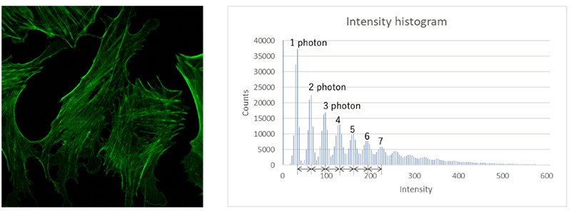
Figure 13. Fluoresces image acquired by FV4000 SilVIR and its pixel intensity histogram. Histogram shows comb shape frequency distribution of detecting photons discretely.
5. SilVIR detector example images
This section presents LSM images captured using the SilVIR detector.
Comparison to images captured using a GaAsP-PMT
Figure 14 shows images of green fluorescence captured by the SilVIR and GaAsP-PMT detectors. The sample was excited by same laser power to achieve typical fluorescence intensity. When the intensity is relatively strong—about 128 photons—both images have similar image quality, but the SilVIR detector has a direct photon count statement.
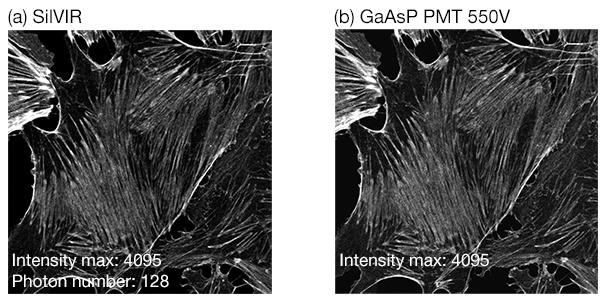
Figure 14. Both the SilVIR and GaAsP-PMT detectors can acquire a bright sample image with an equivalent signal-to-noise ratio. Figure 14(a) was acquired using the SilVIR detector while 14(b) was acquired by the PMT at 550 V. The same sample was excited using the same laser power. The maximum fluorescence intensity is about 128 photons/2 µs.
Scanner: galvanometer scanner, 2 µs/pixel
Excitation: 488 nm laser
Emission: 500 – 540 nm
Actin filaments (BODIPY FL) of BPAE cell
However, the same is not true for weak fluorescence. Figure 15 shows the same sample with weak fluorescence—about 12 photons—captured using the two detectors. You can see that the images captured using the SilVIR detector have less noise than the one captured using the conventional GaAsP-PMT. In addition, the intensity histogram of the SilVIR image is comb-like, indicating that the number of photons was accurately detected in each pixel. On the other hand, the intensity histogram of the GaAsP-PMT image shows that the image intensity is random, which results in a lack of photon quantification. In addition, the high voltage needs to be adjusted according to the strength of the fluorescence to be detected for the GaAsP-PMT, but not for the SilVIR detector.
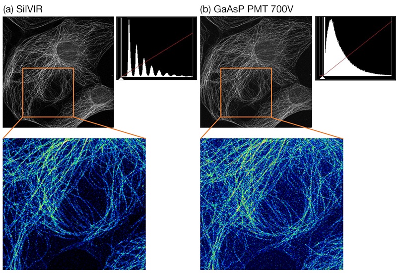
Figure 15. This figure shows a sample with very dim fluorescence captured (15a) by the SilVIR detector and by a (15b) GaAsP PMT at 700 V. The same sample was excited by the same laser power. The maximum fluorescence intensity is about 12 photons/2 µs. The intensity histogram of the image captured using the SilVIR detector shows a comb-like structure, which indicates the number of photons were accurately detected. More noise was observed in the background of the image acquired using the PMT.
Scanner: galvanometer scanner, 2 µs/pixel
Excitation: 488 nm laser
Emission: 500 – 540 nm
Microtubules (Alexa Fluor 488) of PtK2 cell
High signal-to-noise images of resonant scanners using a SilVIR detector
The SilVIR detector is well suited for imaging low-intensity fluorescence. In particular, when acquiring images using a resonant scanner, it is difficult to acquire images with a high S/N ratio because the number of detected photons is very small due to the extremely short pixel-dwell time. The SilVIR detector overcomes this. Figure 16 is an image captured with a resonant scanner at 1024 × 1024 pixels. Images with a different number of averaging are lined up. Even if the number of detected photons is several photon levels, a resonant scanner image with good image quality can be obtained, and a small number of averaging (or accumulations) can process the resonant scanner image to be equivalent quality to the galvanometer scanner image. This also increases image acquisition efficiency.
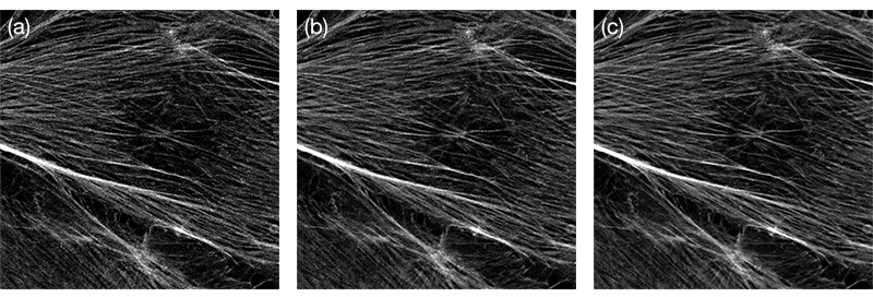
Figure 16. Images acquired using the SilVIR detector and a 1K resonant scanner. Figure 16(a) shows no averaging in the 130 msec/frame, 16(b) shows two times averaging 262 msec/frame, and 16(c) is four times averaging 522 msec/frame. Since the SilVIR detector can acquire high signal-to-noise ratio images using a resonant scanner, the small amount of averaging is enough to obtain a high-quality image. This improves the image acquisition efficiency.
Resonant scanner: 1024 × 1024 pixels one way, pixel dwell time: 0.033 µs
Maximum fluorescence intensity: about 20 photons.
Efficiently acquire stitched images using the SilVIR detector
To acquire a wide-area, high-resolution image, image stitching is often used. This process is slow using a galvanometer scanner, but using the SilVIR detector paired with a resonant scanner makes this process much more efficient. In Figure 17, the four-channel, 1K × 1K-pixel images were acquired at eight Z slices in a 5 × 5-mosaic field. Using a galvanometer scanner, capturing the image took more than 30 minutes, while using a resonant scanner, it took less than 6 minutes.
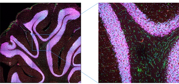
Figure 17. Efficient image acquisition using the SilVIR detector. A maximum intensity projection of stitched Z slice images was acquired using a resonant scanner. Because of the SilVIR detector’s high S/N ratio, a large number of images can be acquired efficiently.
Acquiring high dynamic range images using the SilVIR detector
Dynamic range is limited in conventional PMT imaging; if the sample has a mix of dark and bright objects, one of them must be prioritized. For example, in Figure 18, when acquiring an image of neurons, intensity saturation at the cell body was inevitable to acquire clear images of the neural fiber’s structure with weak fluorescence. The SilVIR detector can acquire both bright and dark areas without saturation thanks to its 16-bit dynamic range.
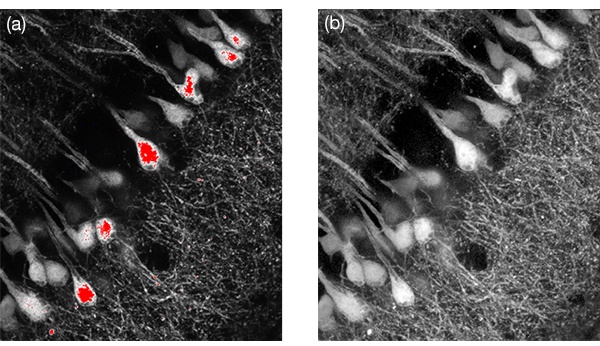
Figure 18. High dynamic range imaging using the SilVIR detector. Figure 18(a) shows a conventional image where some brighter cell body easily got saturated while 18(b) shows an image captured using the SilVIR detector where both cell body and neural fibers were in the detection range. Dim neural fibers were enhanced by adjusting the gamma display.
Multi-color imaging with the SilVIR detector
Taking advantage of the SilVIR detector’s high sensitivity and S/N ratio from the visible to near infrared, six-color-simultaneous imaging is possible while avoiding the effects of crosstalk (Figure 16). Fluorescent dyes excited by 730 nm can hardly be imaged using a GaAsP-PMT detector, but the SilVIR detector can acquire high S/N ratio images. The FV4000 confocal microscope can be equipped with an up to six-channel detector, enabling simultaneous imaging of six colors with a nanometer-precise spectral resolution reaching from 400 to 900 nm.
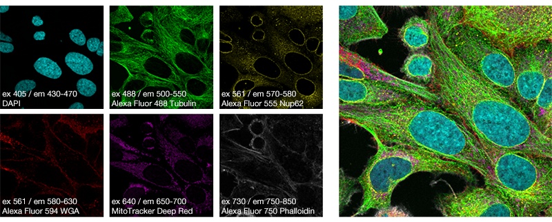
Figure 19. A simultaneous six-color image captured using the SilVIR detector and TruSpectral technology. Simultaneous multicolor imaging from visible to the near-infrared is possible.
6. Conclusion
Compared to conventional detectors, the SilVIR detector offers many benefits, including:
- Multicolor imaging with high sensitivity and high S/N ratio from the visible to near infrared wavelength range.
- High photon detection resolution (high-speed and high dynamic range photon counting).
- High experimental reproducibility based on the quantification of image brightness without sensitivity degradation.
- Simple operation by eliminating the need to adjust the gain as with a PMT.
These benefits make it easier to obtain high-speed, high-resolution images with high S/N ratio while reducing phototoxicity. In addition, since the image brightness can be quantified as the number of photons, sharing and reproducing imaging conditions is easier.
Furthermore, SiPM sensors have great potential for future technological development. For example, FF, which is one of the parameters that determine PDE, may be greatly improved if the microlens array under development for upcoming single photon avalanche diode (SPAD) array sensors and guard-ring-sharing techniques [6] can be successfully deployed. If PDE can be increased, it will be easier to balance the complex tradeoffs between the S/N ratio, dynamic range, speed, and pixel count.
We believe that the SilVIR detector can become the standard for next-generation laser scanning microscopes due to how well it has overcome the challenges associated with conventional detectors and its potential to continue rapid development in the future.
7. References
- Hamamatsu Photonics “Photomultiplier Tubes: Basics and Applications 4th Edition” (Hamamatsu Photonics, 2017).
- Hamamatsu Photonics “MPPC®” Cat. No. KAPD9005E04 (Hamamatsu Photonics, 2022).
- J. Zheng, et al. “Dynamic-quenching of a single-photon avalanche photodetector using an adaptive resistive switch” Nat. Communications 13, Article number 1517 (2022).
- J. Friedrich, P. Zhou, L. Paninski “Fast online deconvolution of calcium imaging data” PLoS Comput. Biol. 13(3) : e1005423 (2017).
- Evident corporation, US Patent No. US11237047B2
- K. Morimoto, E. Charbon “High fill-factor miniaturized SPAD arrays with a guard-ring-sharing technique” Opt. Express 28(9/27), 13068–13080 (2020).
8. Explanations of technical terms
External photoelectric effect: When a metal or semiconductor is exposed to light, electrons in the metal or semiconductor jump to the outside (vacuum space) due to the energy of the light.
Internal photoelectric effect: A phenomenon in which as a semiconductor or insulator is irradiated with light, it increases the conduction of electrons in the material's interior, and the electric conductivity caused by this phenomenon increases.
Geiger mode: The condition where an avalanche photo diode (APD) operates by applied voltage that causes Geiger discharging.
Breakdown voltage: When a certain voltage or more is applied to an APD, a certain level of signal-output inherent to the light-receiving element is generated (Geiger discharging) by light incidence regardless of the amount of light. The breakdown voltage is the minimum applied voltage that causes this.
Dark count noise: Noise when light is not incident.
Crosstalk noise: Pulsed noise generated by photoelectron leakage from neighboring SiPM pixels.
After-pulse noise: Pulse noise delayed in response to the original photon-detection pulse.
Paralyzed model photon count detection: Single photon count detection when one pulse cannot be separated when the photon detection pulses are continuously overlapped. Example: photon counting using a PMT.
Non-paralyzed model photon count detection: Single-photon count detection when the photon detection pulses overlap, but the signal is output at pulse pair resolution intervals. This is equivalent to using a SiPM as a detector.
Pulse pair resolution: Minimal time-interval at which photon detection pulses can be separated in single-photon count detection.
Author
Hirokazu Kubo
Advanced Technology, R&D, Evident Corporation
Productos usados para esta aplicación
Sorry, this page is not
available in your country.