Interference Filters for Fluorescence Microscopy
The performance of high-resolution fluorescence microscopy imaging systems and related quantitative applications, especially as applied in living cell and tissue studies, requires precise optimization of fluorescence excitation and detection strategies. Fluorescence microscopy techniques could not have advanced so dramatically without significant developments in every dimension of the current state of the art, including the optical microscopes, the biology and chemistry of fluorophores, and perhaps most important, filter technology. The utilization of highly specialized and advanced thin film interference filters has enhanced the versatility and scope of fluorescence techniques, far beyond the capabilities afforded by the earlier use of gelatin and glass filters relying on the absorption properties of embedded dyes.
Current techniques in biological research microscopy have become increasingly oriented toward highly specific, sensitive, and versatile localization of fluorescent molecular probes in small numbers, with the ultimate goal of determining their role in cellular and molecular processes. In the widefield epi-fluorescence illumination configuration, the optical filter combination plays a critical role in maximizing signal-to-noise ratio, and thereby aiding the microscopist in balancing the conflicting requirements of enhancing fluorochrome excitation, while simultaneously limiting photobleaching and cell phototoxicity. The classical epi-fluorescence microscope is characterized by partially coincident excitation and detection optical pathways, requiring the filter complement employed to reduce the intense excitation light, following specimen interaction, by a factor ranging between one and ten million in order to allow practical image formation from the often-limited number of emitted fluorescence photons. Highly effective fluorescence filter sets are necessary in order to provide maximum attenuation of excitation light in the detection pathway, in parallel with the successful capture of as many emitted photons as possible. Very high detection efficiency for fluorescence emission enables a corresponding reduction of the overall illumination level, which minimizes photobleaching of fluorochromes and phototoxicity to the specimen.
High performance filters based on optical interference phenomena have helped to revolutionize the application of fluorescence techniques in widefield and confocal microscopy. Much of the current progress for improving specificity of fluorescence labeling is due to the development of techniques that enable antibody conjugation with a variety of synthetic fluorescent probes. In combination with carefully tuned chemical characteristics for the fluorochromes and enhanced sensitivity due to the better signal-to-noise ratio afforded by optical advances in interference filters, the resolution limit of current fluorescence techniques extends to the visualization of single molecules.
Interference filters are constructed by depositing thin layers of specialized materials onto flat substrates. Their design relies on thin-film deposition and thin-film optical interference technologies, both of which are crucial in modern optical component design, as well as in the semiconductor and optical communications fields. The basic structure of an interference filter features alternating layers of high and low refractive index materials, each typically an integral multiple of one-quarter wavelength in thickness. By careful selection of thickness and refractive index values for the various layers, which are usually deposited on a glass or fused silica/quartz substrate, controlled interference of light waves reflected at each layer interface can be utilized to enable the filter to reflect specific wavelengths while transmitting others. Although the layers are themselves colorless, the fluctuation in conditions required for constructive and destructive interference as a function of wavelength results in the appearance at the filter surfaces of varying interference colors, similar to those seen in color swirls on a soap bubble surface.
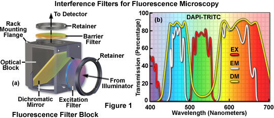
The basic filter complement required for classical fluorescence microscopy utilizing widefield episcopic illumination, as well as for many laser scanning confocal techniques, comprises three separate elements that are typically combined into one optical mount, commonly referred to as a filter cube or block. The filter components include an excitation filter, a dichromatic mirror (or beamsplitter), and an emission (or barrier) filter, as illustrated in Figure 1. Each component performs a different specific function, but all are enhanced by precise utilization of interference effects. Characteristics of the three optical filter elements and the necessary performance specifications for each are discussed in more detail in the following sections. In general, the selection of an optimal filter set for a particular investigation requires a thorough consideration of the spectral interactions between the filters and the fluorochromes, the microscope illumination source, and the detector employed to capture the signal.
A typical fluorescence filter set along with the visible region spectral profiles of the component interference filters is presented in Figure 1. The dichromatic mirror is mounted at a 45-degree angle with respect to the optical axes of the filter block and secured into place with cement or miniature clamps. The excitation and barrier filters are placed into seats on the front and top faces of the block and locked into position with circular retaining rings (Figure 1(a)). Light from the microscope illuminator enters the block through the excitation filter, and secondary fluorescence emission exits the block through the barrier filter. The spectral profile of this filter set is illustrated in Figure 1(b). Designed for simultaneous imaging of fluorophores responding to ultraviolet and green excitation wavelengths, this combination contains an excitation filter having two bandpass regions (380-420 and 510-560 nanometers). Note that transmission values for the ultraviolet excitation profile are lower than those of the green profile, due to greater absorption by the filter coating materials at wavelengths lower than approximately 400 nanometers. The dichromatic mirror has two regions of high transmission to accommodate corresponding transmission regions in the emission filter. Also, similar to the excitation filter, the barrier filter has two bandpass regions and is designed for simultaneous observation of blue and red fluorescence emission.
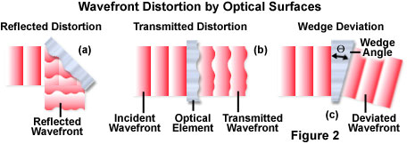
Illustrated in Figure 2 are three of the fundamental parameters most often employed to gauge the optical quality and performance of filters. The surface flatness (Figure 2(a)) is a measure of the deviation from a perfectly flat or planar surface, and is calculated in fractions or multiples of an average wavelength (usually 550 nanometers). Wavefront distortion produced by reflection from an irregular surface is twice the value of the surface flatness. This parameter is critical in determining the quality of dichromatic mirrors, which reflect excitation illumination from the front surface in fluorescence microscopy. The distortion of a plane wavefront passing through the filter is termed transmitted distortion (Figure 2(b)), and is also measured in fractions or multiples of a wavelength. Contributing to the transmitted distortion artifact is the flatness of the outer surfaces, as well as refractive index fluctuations produced by internal defects. Angular deviation from parallelism between the outer filter surfaces is referred to as wedge (Figure 2(c)), which is measured in arc-seconds or arc-minutes of the deviation angle. Image shifting due to beam deviation is the most problematic artifact caused by excessive filter wedge angles in fluorescence microscopy. For a typical filter, the magnitude of deviation is approximately equal to one-half the wedge angle. In addition to image shifting, wedge defects can produce ghost images from off-axis internal reflections.
The primary function of the excitation filter is to block all light from the illumination source except for a selected band of wavelengths that corresponds to the absorption characteristics of the fluorochrome used to label the specimen. The absolute requirements differ somewhat in accordance with the light source being employed. If broad-range sources such as mercury or xenon arc-discharge lamps are used, most of their output, which ranges from the ultraviolet to near-infrared wavelengths, must be excluded from reaching the specimen. In many circumstances, the appropriate excitation filter has a limited bandpass transmission range of approximately 40 nanometers (full-width at half-maximum; FWHM), centered on the absorption maximum of the fluorophore. An interference filter of this type is constructed with multiple dielectric layers deposited onto float glass and sealed with an epoxy laminate to protect the hygroscopic thin film layers from moisture. Although generally designed to be positioned perpendicular to the beam path (at zero degrees incidence), many filter optical block designs tilt the excitation filter a few degrees in the mounting seat in order to minimize interference from internal reflections. Precautions taken to limit reflections are particularly important when laser illumination is employed because of the potential for high intensity reflections to damage the laser cavity.
Due to the fact that the excitation filter element is not positioned in the fluorescence emission image-forming pathway, the highest degree of optical precision is not required. Excitation filters typically have a design tolerance of less than approximately six arc-minutes of wedge, but more precise grinding and polishing is not required. It is essential, however, that the coating layers, as well as any epoxy laminates applied as protective layers, are free of defects such as inclusion of foreign materials or bubbles. Pinholes in the coating layers must also be eliminated since they allow undesirable wavelengths to pass through the filter and diminish the signal-to-noise ratio of the imaging system.
The dichromatic beamsplitter is positioned between the excitation and emission (barrier) filters at an angle of 45 degrees to the beam path (see Figure 1). Traditionally, this optical element has been referred to as a dichroic mirror, and serves two primary functions in the episcopic illumination configuration. Designed as a specialized longpass filter, the dichromatic beamsplitter utilizes interference layers to reflect certain wavelengths and transmit others, and therefore functions to separate wavelengths on opposite sides of a narrow boundary having limited wavelength range. Placed at a 45-degree angle to the optical axis, the dichromatic beamsplitter reflects shorter excitation wavelengths at a 90-degree angle and passes them along the illumination axis to the specimen. Simultaneously, this critical element transmits longer fluorescence wavelengths emitted by the fluorophores, which are then collected with the objective and imaged by the detector.
The design requirements for a dichromatic mirror must account for the fact that it plays a role in both the excitation and emission light paths. The coatings are selected to produce minimal autofluorescence, as is the substrate material, which typically consists of fused silica or quartz. By taking advantage of sophisticated interference filter design techniques, the transition from near total reflection to maximum transmission can take place over a very short wavelength range, enabling precise discrimination of excitation and emission light. In addition to displaying well-defined spectral characteristics, the physical tolerances of this optical component are very strict. Published specifications commonly state a requirement of less than 1 arc-minute of wedge, a surface flatness deviation of less than 10 wavelengths per inch (affecting the reflected beam), and a transmitted wavefront distortion of 1 wavelength per inch or less (affecting the transmitted emission signal). It is important to note that there are limits on both the reflection and transmission ranges of dichromatic mirrors, and that the transition cannot be made precisely at a specific wavelength, but takes place over a narrow range of wavelengths. The dichromatic beamsplitter does not reflect all wavelengths below the transition region with 100-precent efficiency, and will begin to transmit again at lower wavelengths. Similarly, the transmission characteristics are not perfectly uniform on the long wavelength side of the transition. In many cases, transmission typically either falls off at wavelengths longer than the design range, or exhibits other irregularities in the deep red and near-infrared regions.
The third component of the standard fluorescence microscopy filter set is the emission, or barrier, filter. This optical element is primarily required to block light from the excitation wavelengths, and secondarily to pass only the desired spectral portion of fluorescence emission to the detector. The optical characteristics of the emission filter must be carefully matched to those of the excitation filter in order to achieve the level of excitation wavelength rejection necessary to allow the relatively weak fluorescence emission signal to be recorded. The excitation light in common fluorescence techniques can be more than a million times brighter than the emission from the fluorochrome, and even a relatively minor amount of unblocked excitation illumination can completely overwhelm the signal. Typically, emission filters are designed to block wavelengths from a specific corresponding excitation filter to an optical density level of 5.5 or greater.
In effect, the emission filter functions as a second stage to remove excitation light that is incompletely blocked by the dichromatic beamsplitter, and also serves to regulate the noise level of secondary fluorescence emitted by the specimen. In the most accurate fluorescence filter sets, the emission filter is a bandpass style matched to the emission spectrum of the fluorochrome, although in some applications a longpass filter is employed to collect a larger signal. Longpass emission filters have the disadvantage of passing more interference from other fluorochromes and/or autofluorescence, thus, as a consequence, most high-resolution techniques utilize bandpass filters. This filter design maximizes the signal-to-noise ratio in applications for which spectral discrimination of signal components is more important than overall intensity. Interference emission filters must be ground and polished to a high degree of precision, with specifications similar to those of dichromatic mirrors: less than 1 arc-minute of wedge and with a transmitted wavefront distortion beneath 1 wavelength per inch. It has become common to tilt this optical element a few degrees with respect to the microscope optical axis, as is often done with the excitation filter, in order to minimize internal reflections.
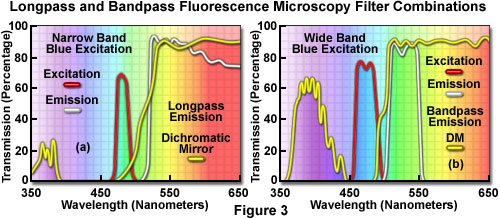
Presented in Figure 3 are typical longpass (Figure 3(a)) and bandpass (Figure 3(b)) filter combinations designed for routine duty in fluorescence microscopy. The longpass filter set contains a 20-nanometer bandpass excitation filter with a 480-nanometer center wavelength, which is considered a narrow passband range. The dichromatic mirror and barrier filter have a cut-on wavelength of 500 and 520 nanometers, respectively. Utilizing longpass barrier filters increases the signal level over that obtained with bandpass filters. The 30-nanometer wide band excitation filter in the bandpass fluorescence set (Figure 3(b)) provides more excitation energy than does the narrow counterpart in the longpass set (Figure 3(a)). However, the restricted region for signal detection imposed by the bandpass barrier filter (40 nanometers in this case) reduces the overall fluorescence intensity reaching the detector.
Interference Filter Principles
The evolution of thin-film technology for filter production has dramatically improved the versatility of spectral control in optical microscopy. Early filter designs consisted of colored dye solutions chambered in cuvettes, followed sequentially by dye-containing gelatin sheets, gelatin-glass combinations, and solid colored glass filters. Such filters, which rely on absorption to attenuate light, are durable and inexpensive, but their usefulness is limited by low peak transmittance, poor wavelength discrimination, and often, high levels of autofluorescence. Thin-film coatings of metallic materials for fully reflective mirrors and neutral density filters, as well as transparent interference coatings for wavelength selection, are widely used devices for light control. Currently, interference filters can be produced with very precise specifications, allowing their optical performance to be optimized for most applications. Utilizing thin-film coating techniques, a wide variety of filter designs can be fabricated, including longpass or shortpass edge filters, narrow or broad bandpass filters, multiple bandpass filters, and dichromatic beamsplitters.
Interference filters are multilayer thin-film devices. Their optical properties are derived from the principles that govern reflection and transmission of light at the interface between two dissimilar media. These principles can be easily extrapolated to the behavior of light interacting with a single thin film deposited on a substrate of different composition, and similarly to multiple thin-film layers of variable composition and thickness deposited in structured stacks on a substrate. Interference filters are typically fabricated by vacuum deposition of metallic salt thin films on an optical glass substrate. If the process is repeated using several different film materials, a multilayer filter is produced, providing multiple interfaces at which light is reflected or refracted.
Reflection of incident light at an air-glass interface is an important concept that regulates the action of lenses, filters, mirrors, and other optical components in the microscope. When light encounters a transparent glass surface, approximately 4 percent of the total incident radiation is reflected. Consequently, a stack of eight glass elements transmits approximately 50 percent of the incident light, with the remainder being reflected at the 16 glass surfaces (the front and rear of each element). An analogous effect is produced by multiple thin-film coating layers applied to a glass substrate. Fortunately, the thickness and refractive index of each layer can be carefully selected in order to control the reflection and transmission characteristics of specific wavelengths at the interfaces. The layered structure can therefore be exploited to produce either constructive or destructive interference (or an intermediate combination of the two processes) between the wavefronts reflected by each interface to selectively generate preferred reflection or transmission for certain wavelength ranges.
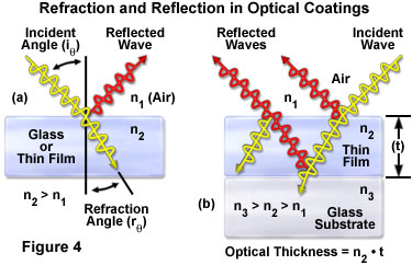
The critical physical phenomenon regulating the construction of interference filters is the reflection that occurs when light is incident upon a smooth interface between two transparent media. Reflection characteristics at such an interface depend on the refractive indices of the two materials, the angle of incidence, and the polarization orientation (if any) of the incident light. When light is incident upon the interface, a fraction of the light enters the second medium and is refracted, while another portion is reflected at the interface (see Figure 4). The relationship between the angle of incidence (i) and the angle of refraction (r) for two media having refractive indices n(1) and n(2), as illustrated in Figure 4, is given by Snell's Law:
n1 • sin(i) = n2 • sin (r)
With reference to the angles of incidence and refraction (i and r), the reflectance for the two polarized light components at the interface is dictated by the following expressions:
Rp = [(n2 • cos(i) - n1 • cos(r)) / (n2 • cos(i) + n1 • cos(r))]2 Rs = [(n1 • cos(i) - n2 • cos(r)) / (n1 • cos(i) + n2 • cos(r))]2
in which R(p) is the reflectance of light polarized parallel to the plane of incidence, referred to as p-polarized light, and R(s) is the reflectance of light polarized perpendicular to the plane of incidence, or s-polarized light. At normal incidence, the polarization differences do not occur, and the total reflectance (R) is equivalent to the reflectance of the s and p components, as expressed by the equation:
R = Rp = Rs = [(n2 - n1) / (n2 + n1)]2
Considering this relationship, for light waves passing through air (whose refractive index is 1.0) and into glass optical elements having a refractive index of 1.5, reflectance (R) is 0.04 for each air-glass surface, or 0.08 for two surfaces at normal incidence. In the previous example of eight stacked glass elements, the transmittance through the 16 surfaces is 0.96 to the 16th power, or approximately 52 percent (equivalent to a 48-percent reflection loss). The reflectance equation dictates that for glass elements in air (n(1) equal to 1.0), the reflectance increases with increasing values of n(2). The high loss to reflection from uncoated glass elements emphasizes the potential benefit that can be derived from incorporating effective antireflection coatings on optical elements. An additional factor that is critical in the function of optical coatings, particularly for interference filters, is that when light propagates across an interface, such as that illustrated in Figure 4(a), if n(2) is greater than n(1), the reflected wave undergoes a phase change of 180 degrees.
The variation in reflectance that is generated by refractive index mismatches between two adjoining media, combined with the phase changes that occur upon reflection, provide a mechanism by which optical interference can be exploited to modulate the transmission and reflection of desired wavelength regions by an optical element. By depositing thin layers of transparent dielectric materials onto a glass substrate, the reflection and transmission of specific wavelength ranges can be controlled without a significant loss of light intensity. With appropriate choice of dielectric refractive index, layer thickness, and the number of layers, the spectral properties of interference optics can be customized over a very broad range.
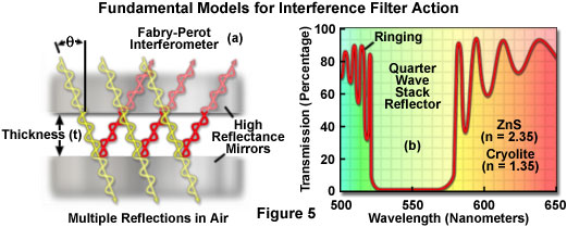
Whether designed to function as an edge filter or a bandpass filter, multilayer thin-film devices perform wavelength selection through the phenomena of both constructive and destructive interference. They are based on the same principles, and in most cases can be categorized, as Fabry-Perot interferometers (Figure 5(a)). These simple interferometers rely on interference among multiply reflected wavefronts to transmit a selected wavelength range while blocking all other wavelengths. The operating mechanism in this type of filter is best described by first considering the simple example of monochromatic light incident on a single thin-film dielectric coating on a glass substrate, with the thin film having an index of refraction intermediate between that of air and the glass. The three dielectric materials, having refractive indices n(1), n(2), and n(3), are illustrated in Figure 4(b). The thin film has thickness t, and separates materials of semi-infinite thickness.
In the configuration described by Figure 4(b), some reflection occurs at each interface, and is often referred to as the Fresnel loss (or Fresnel reflection, named after Augustin Fresnel). The proportion of incident light reflected can be determined from the equation for total reflectance (R), which upon analysis reveals that the Fresnel loss becomes greater as the refractive index difference across the interface (n(2) - n(1)) increases. As light propagates through the thin film and into the third medium, a logical assumption would be that the transmitted intensity is reduced by the sum of the Fresnel losses occurring at the two interfaces. However, if the film thickness is small (on the order of the light wavelength), interference occurs between waves reflected from the two surfaces, which can either increase or reduce the total combined intensities. The nature of the interference depends upon the phase relationships of the wavefronts following reflection at each surface, and this in turn, depends upon the wavelength, the refractive indices of the materials, and the incidence angle.
If the thin-film refractive index, n(2), is intermediate between that of air and the substrate, incident light reflections occur at the air-film interface and the film-substrate interface, as illustrated by the red waves in Figure 4(b) (note that the angle of incidence is dramatically exaggerated). The phase relationships between the rays reflected from the interfaces are determined by the thickness of the film relative to the wavelength of light and the comparative values of the refractive indices. Because n(2) is greater than n(1), light waves reflected from the first surface (the thin-film surface) exhibit a 180-degree phase change. If the film thickness is selected such that the optical thickness (the product of thickness, t, and refractive index, n(2)) is equal to one-quarter of the light wavelength (λ/4), the ray propagating through the film and reflecting from the film-glass interface undergoes a 180-degree (λ/2) phase change upon reflection. In addition, a second 180-degree phase change occurs upon return of the wave through the thin film. The net full-wavelength phase change for this ray compared to the half-wavelength phase change of the first reflected ray results in a 180-degree phase difference between the two reflected rays, and produces destructive interference. With the reflected rays being effectively cancelled, a thin film of quarter-wave thickness functions as an anti-reflection optical coating. Longpass and shortpass filters employing multiple thin films in their structure will, if properly designed, display anti-reflection characteristics.
The phase relationship between the two reflected rays can be altered simply by utilizing a thin-film material of different refractive index. Applying the same configuration as described above, but instead with a thin-film refractive index greater than that of the substrate (as well as that of air), the first reflection will generate the same 180-degree phase change. The ray propagating through the film, however, does not change phase upon reflection, since n(2) is now greater than n(3), and only acquires the normal 180-degree phase lag (λ/2) associated with a double journey through the quarter-wave-thick (λ/4) film. Constructive interference occurs between the two reflected wavefronts (each with a 180-degree phase change), thus increasing the reflectance in comparison to that from the lower refractive index thin-film coating, and causing the optical element to function as a partial reflector.
By utilizing thin-film interference technology, a wide range of useful devices can be fabricated. As is obvious from the previous discussion, thin-film coating properties can be fine-tuned to take advantage of superimposition by multiply reflected wavefronts. The nature of interference phenomena between the waves can be purely constructive, destructive, or one of many intermediate phase relationships. Considering the example of the anti-reflection coating structure, if the optical thickness of the film is not an integral multiple of one-quarter wavelength, the two reflections are not exactly 180 degrees out of phase. Consequently, interference is not totally destructive, resulting in reflectance that exceeds the theoretical minimum. Other phase relationships may be utilized to manipulate the transmission and reflection properties of thin-films. Dielectric thin-film layers of one-half wavelength thickness produce a phase change of 360 degrees (a full wave), and can function as an absentee layer with no effect on reflectance or transmission for a specific design wavelength. For structures consisting of only dielectric materials, the combined transmitted and reflected ray energies are equal to the incident light energy.
Interference Filter Design
The composition and arrangement of thin-film layers deposited on a filter substrate determine the transmission and reflection properties of the device. When light waves having equal wavelength occupy the same physical space, they interfere with each other in a manner determined by their relative phase and amplitude. The interference is destructive if the waves are exactly out of phase (by 180 degrees), and if their amplitudes are equal, they cancel each other to yield a wave of zero amplitude. When two waves are exactly in phase with each other, they interfere constructively to generate a wave of larger amplitude. Thin-film optical coatings composed of multiple layers are designed so that the optical distances between the layer boundaries (usually integral quarter-wavelength multiples) control the phase differences of the multiply reflected and transmitted light waves. Successively applied layers in the optical coating effectively constitute a stack of boundaries, each of which produces reflected and transmitted components that are subsequently reflected and transmitted from the other boundaries. Polychromatic light propagating through such a multiple-layer structure will be subject to destructive interference and attenuation at specific wavelengths, and constructive interference with enhanced transmission at other wavelengths.
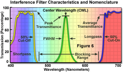
Coating performance characteristics are influenced by the number of boundaries in the layered structure, the refractive index differential across each boundary, and the distances between the boundaries within the coating. Manufacturers of interference filters apply optical thin-film theory with the aid of specialized design software to optimize the characteristics for specific applications. By varying the thin-film structure, filter performance specifications can be controlled with a great deal of precision. Among the characteristics that are manipulated through thin-film design are the degree of transmission and reflection, the extent of the spectral range over which transmission and reflection (and intermediate transitions) occur, and the polarization effects at off-normal angles of incidence. Presented in Figure 6 are the critical spectral characteristics and nomenclature commonly employed to describe interference filters. Included are locations for the peak and average transmittance values, as well as the center wavelength (CWL) for bandpass filters and the cut-on and cut-off values for shortpass (yellow curve) and longpass (blue curve) filters, respectively. The blocking range for the bandpass spectral profile (green curve) in Figure 6 is also indicated.
As discussed previously, quarter-wave dielectric layers can be designed to function as anti-reflection coatings on glass substrates, or alternatively, to constructively enforce reflection. The quarter-wave stack reflector (see Figure 5(b)) is composed of alternating layers of two or more dielectric materials, and is utilized as a basic building block for optical thin-film devices. The design optical thickness of each layer is satisfied for only one particular wavelength value, which is referred to as the principal wavelength of the device. The quarter-wave stack reflector spectral profile illustrated in Figure 5(b) was obtained from a device consisting of twenty-three layers alternating between zinc sulfide (refractive index of 2.35) and cryolite (refractive index of 1.35) on a glass substrate, with a principal wavelength of 550 nanometers. A slight design modification could be employed to eliminate the dips (often referred to as ringing) in the transmission regions, optimizing the element for use as a longpass or shortpass cut-on filter. A coating of this composition exhibits the highest reflection at the principal wavelength, and transmits wavelengths that are higher and lower than the principal value. The coating performance is the result of constructive interference of reflected waves at the principal wavelength as well as minimized overall transmission due to destructive interference between transmitted waves. Quarter-wave stack reflectors are suitable for utilization as rejection band filters, blockers, and cut-on filters.
Narrowband interference (bandpass) filters operate under the same principles as the Fabry-Perot interferometer, relying on the interference between multiple reflected beams. In a typical Fabry-Perot interferometer (constructed for spectroscopic applications; see Figure 5(a)), incident light undergoes multiple reflections in a central transparent (air) medium located between two reflective surfaces. Each transmitted wavefront undergoes an even number of reflections between the surfaces that define the interferometer cavity. Phase differences between emerging wavefronts determine whether a transmission maximum occurs or, instead, most of the light is reflected back toward the source. The wavelength region for which a particular condition prevails, for a given incidence angle, depends upon the optical thickness of the region separating the reflectors, which for air (n equal to 1.0) is equal to the physical thickness.
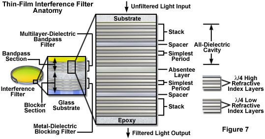
The simplest bandpass filter based on interference principles is a thin-film solid Fabry-Perot interferometer, often referred to as a cavity or a single-cavity coating. Typically, these filters are constructed by separating two thin-film reflectors with a thin-film spacer (as illustrated in Figure 7). In an all-dielectric cavity, the conventional air gap is replaced by a thin layer of dielectric material having an optical thickness equivalent to an integral half-wavelength of the principal design wavelength (the desired transmission peak). The thin-film high reflectors are normal quarter-wave stack reflectors having a broadband reflectance that peaks at the principal design wavelength. The spacer separating the reflectors, due to its half-wavelength thickness, induces transmission rather than reflection at the principal wavelength and consequently supports multiple reflections within the cavity. Light of longer or shorter wavelength than the principal wavelength acquires a phase difference that maximizes reflection and minimizes transmission. This combination of interference phenomena produces an effective bandpass filter. Properties of the filter, such as width of the passband region, level of transmission within the passband, and the blocking range outside that spectral region, are determined by the number of layers and their arrangement. A narrow passband, which is often a design goal for this type of filter, is achieved by increasing both the reflectance of the quarter-wave stacks comprising the cavity and by increasing the thickness of the thin-film spacer.
A wide spectrum of variation is possible in the detailed structure of interference filters. Although many are constructed entirely of dielectric materials, it is common for broadband interference filter designs to include a metallic layer in the spacers. Even in all-dielectric filters, metallic thin-film layers are typically incorporated in auxiliary structures that serve as blocking filters for certain spectral regions (Figure 7). Metal-dielectric-metal (MDM) cavities may be employed in applications involving filtration of ultraviolet light, which would be completely absorbed by all-dielectric structures. In this type of solid Fabry-Perot interferometer, the reflectors are metallic thin-films separated by a spacer layer of dielectric material having integral half-wavelength thickness.
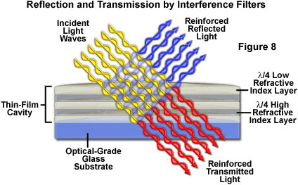
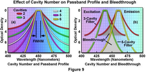
The typical quarter-wave stack reflector, as discussed above, is constructed from alternating layers of high refractive index and low refractive index dielectric materials (see Figures 7 and 8). A pair of high and low-index layers constitutes the simplest period, which is typically repeated multiple times in constructing a stack having the desired performance characteristics. The combination of two stacks with an appropriate spacer layer constitutes a single-cavity filter. Two or more such cavities can be coupled with a matching (absentee) layer to form a multi-cavity passband filter. Figure 7 illustrates the detailed structure of a typical two-cavity passband interference filter. The overall transmission passband that results from a multiple-cavity structure is approximately equivalent to the product of the values for the individual cavities. Consequently, as the number of cavities increases, the cut-off edges of the passband slopes become steeper and the reflectance outside the passband increases (see Figure 9), producing improved rejection of wavelengths adjacent to the passband region. The steeper edge slopes produce passband peaks that are nearly square rather than Gaussian or Lorentzian in shape, a characteristic considered advantageous for certain filter designs.
In the nomenclature of optical thin-film technology, it is common to symbolize a quarter-wavelength optical thickness layer of a high-index material with the letter H, and to designate a quarter-wavelength optical thickness layer of low-index material as L (Figures 7 and 8). Various exponential and fractional designations in combination with the letters are utilized to represent the number of periods and the optical thickness of the stack layers. Often, the terminology designating interference filter construction is specific to each manufacturer. Zinc sulfide is a commonly used high-index material, while cryolite, a naturally occurring sodium aluminum fluoride mineral, is typically employed for the low-index layers. The spacer layer is a half-wavelength thick film of high-index material, and the absentee (coupling) layer is composed of low-index material having a half-wavelength thickness.
As previously mentioned, the number of cavities employed in the design of a bandpass interference filter influences the ability of the filter to discriminate between in-band and out-of-band wavelengths. Figure 9(a) presents typical transmission profiles as a function of wavelength for several theoretical filters constructed with different numbers of cavities. At an equivalent bandpass and center wavelength, as the number of cavities is increased, the degree of light attenuation outside the passband is greater at wavelengths farther removed from the principal wavelength. With a large number of cavities, the transmission passband of the filter approaches the desired square wave profile indicative of a sharp transition between the transmission and attenuation wavelength regions. In practice, this filter characteristic is manifested by improved wavelength discrimination and higher energy transmission efficiency. Bandpass filters with sharp cut-on and cut-off transitions are useful in their ability to effectively separate excitation and emission wavelengths for fluorochromes that exhibit small Stoke's shifts.
The significance of improved wavelength discrimination that results from filter designs employing a large number of cavities is best illustrated by considering the potential effect of bleed-through into an adjacent filter or cavity stack. In practice, this artifact occurs in fluorescence microscopy when excitation energy is transmitted through the emission filter. The result of bleed-through is the undesirable addition of excitation light energy to the signal that is detected as specimen fluorescence, increasing the background level and raising the lower limits of fluorescence detection. Figure 9(b) illustrates typical interference filter transmission curves, using both three and five-cavity designs, which are centered on excitation and emission wavelengths of 435 and 460 nanometers, respectively. With a small difference in excitation and emission wavelengths, the steeper transition of the passband profile exhibited by the five-cavity filter design significantly reduces potential bleed-through as a result of the spectral overlap region occurring at much lower transmission values. In order to obtain acceptable levels of bleed-through utilizing three-cavity filters, the center wavelength of the two filters would have to be selected with additional wavelength separation. For a fluorochrome with a small Stoke's shift, this approach would significantly reduce the efficiency of both fluorescence excitation and detection.
In addition to the fundamental design features described above, matching interference filters to specific applications requires consideration of performance characteristics that are optimized through advanced techniques in filter construction. The functional level attained by a filter in an optical system depends upon how well the design is integrated with other components in the system. Even though an interference filter may meet every primary performance requirement when considered as an isolated component, specific optical system criteria often necessitate the incorporation of other structures into the filter assembly. As an example, filters utilized with a light source or detector that operates over a broad spectral range require a mechanism for extending the attenuation range beyond that provided by a multi-coated single substrate surface. Furthermore, increased attenuation level may be necessary if a very intense illumination source or a highly sensitive detector is employed. Although some optical systems provide sufficient physical space for incorporation of separate absorbing or reflecting elements, these blocking or attenuating components are typically combined with the primary interference coating into a single assembly.
Adding specialized components to filters in order to increase attenuation always results in some transmission loss at the desired wavelengths, and a reduction in total luminous throughput of the system. Consequently, the strategies employed for blocking are devised to provide an optimum balance between transmission and attenuation for the specific application. For example, the blocking might be designed to provide attenuation only over a wavelength range that conforms to the detector's sensitivity, while allowing transmission of light energy outside the detection range.
In bandpass interference filters, such as the two-cavity example illustrated in Figure 7, blocking adjacent to the passband (on the long wavelength side) can be provided by adding multilayer thin-film blocking structures. For the theoretical filter presented in Figure 7, a metal-dielectric hybrid blocking filter performs this function. In typical commercial products having similar design, the multilayer blocking filter limits transmittance on the long wavelength side of the passband to perhaps 0.01 percent. Often, the compromise between greater blocking levels and the accompanying overall transmission loss must be weighed against filter target performance requirements and the greater costs of producing more complex assemblies.
Extended reduction or elimination of unwanted wavelengths can also be achieved through the use of absorbing components that operate by attenuating in specific wavelength regions while continuing to transmit the desired wavelengths. Absorptive colored glass is commonly utilized to suppress transmission on the short wavelength side of an interference filter passband. Such glass elements may either be used as substrates for the interference coatings or laminated onto the filter assembly after fabrication (see Figure 7). Thin-film coating materials, both dielectric and metallic, can also be used to provide attenuation by absorption. In addition to absorptive glass components, dyes can be added to the optical cement during filter assembly to provide a supplemental absorption value to the primary bandpass characteristics of a filter system.
Although absorbing materials are ideal for some blocking and attenuation functions, such as short-wavelength blocking adjacent to a passband, their specifications are not necessarily ideal for every application. In many situations absorbing media do not provide the necessary degree of transmission, absorption level, or cut-off transition profile. Furthermore, these materials are usually susceptible to temperature increases due to their excess absorption of energy, which can result in significant wavelength shifts or physical damage to the optical system.
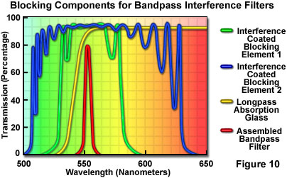
In order to provide a higher level of performance (although at greater cost), dielectric thin-film coatings are commonly employed to extend attenuation throughout the design spectral region. Providing supplementary filtration to the principal interference structure, these additional dielectric coatings can be applied to substrates and laminated to the filter assembly. Several blocking components, which may be longpass, shortpass, or very wide bandpass, can be combined to provide high transmission in the desired spectral region, while simultaneously generating high reflectivity in regions where the primary coating "leaks" unwanted wavelengths. Figure 10 illustrates the spectral characteristics of a principal bandpass filter with the addition of several blocking components to extend the attenuation range. Note that some reduction in transmittance within the bandpass is unavoidable when the light leaks are eliminated in this manner.
Many options are available for customizing interference filter performance. One popular alternative to the use of all-dielectric coatings is to include metal thin-film bandpass coatings. This strategy is simpler in that a single coating element will often extend attenuation into the far-infrared spectral region. The primary disadvantage of metal coatings is that they are absorptive and may reduce transmission in the desired passband to levels between 10 and 60 percent. In contrast, a comparable all-dielectric filter typically allows transmission values of 45 to 85 percent in the passband region.
Two common strategies for extension of single-coated filter attenuation regions are referred to as blocking optimized and blocking complete. Filters designed for optimized blocking are often employed with detectors having limited spectral sensitivity whereas complete blocking is applied to filters used with detectors exhibiting full-range spectral sensitivity. A filter designed to optimize the blocking characteristics combines a colored absorption glass element for the short wavelength side of the passband with a dielectric reflector for the long wavelength side of the passband. The completely blocked filter designs utilize a metal thin-film bandpass coating, which is commonly supplemented with a colored glass component to enhance attenuation of short wavelengths.
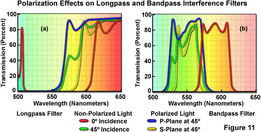
Most interference coatings are designed to filter collimated light at a normal incidence angle (with the coating perpendicular to the light path). Several effects result from light incidence at angles other than normal to the filter surface: the central wavelength shifts to a lower value, which differs for the two orthogonally polarized components, the overall transmittance decreases, and the bandwidth increases. These factors must be taken into consideration by optical designers for components that are intended to be used at significant angles with respect to normal (such as beamsplitters), and by users when filters are not aligned in their intended orientation. The effects of tilt angle are observed for both edge and bandpass filters employing interference coatings. For incidence angles less than approximately 25 degrees from normal, the effect on transmittance and bandwidth can be considered minimal. The wavelength shift is significant, however, and is sometimes exploited to precisely tune the center wavelength of a narrowband filter. The polarization splitting that occurs as incidence angle deviates from normal is extremely important, and although it can be utilized to advantage in some applications, it is generally considered an undesirable property of interference coatings. Angle-dependent polarization is the primary limiting factor that prevents cut-on transitions of 45-degree dichromatic beamsplitters from being as steep as those of edge or bandpass filters used at normal incidence. The polarization effect induced by an interference filter takes somewhat different forms depending upon whether the light incident on the filter is already polarized or is unpolarized prior to being transmitted (discussed further in reference to Figure 11).
The change in properties with filter angle relative to the light path can be understood by considering that interference filters are composed of a series of dielectric layers (and possibly metals) having precisely controlled optical thickness. Increasing the angle of incidence increases the (apparent) optical thickness of the layers, and also decreases the phase difference between the interfering light waves. The shift of transmission and reflectance spectra toward a shorter principal wavelength as incidence angle is increased occurs for both single and multilayer dielectric coatings, as well as for interference filters of more complex construction. With some optical filters (such as dichromatic beamsplitters and bandpass filters), the shift to shorter wavelengths at oblique incidence angles is deliberately employed as a mechanism to fine-tune the principle wavelength. Considering a relatively large tilt angle as an example, a 665LP (longpass) filter (50 percent of peak transmittance at 665 nanometers) performs as a 605LP filter at a 45-degree angle of incidence.
The observed decrease in central wavelength as filters are tilted is a function of the thin film refractive indices and the angle of incidence. By using a single value for the effective refractive index of the interference coating, the relationship between the principal wavelength shift and the angle of incidence is simplified to the following expression for collimated light at angle θ (applicable to angles less than 25 degrees):
λθ = λ0 [1 - (n0/n)2 • sin2(θ)]1/2
where λ(θ) is the principal wavelength at the angle of incidence, θ, and λ(0) is the principal wavelength at normal incidence (zero degrees). The refractive index of the external medium (designated n(0); 1.0 for air) and the effective refractive index for the filter (n) are the remaining variables in the equation.
The effective refractive index of an interference filter is determined by the coating materials and the sequence in which they are deposited, which are factors that can be controlled in the design process. When common dielectric materials, such as zinc sulfide and cryolite are used in construction of standard visible and near-infrared bandpass filters, experimental values of the effective refractive index are typically 1.45 or 2.0, depending upon whether the spacer layer is composed of the low or high refractive index material. The material chosen for the spacer layer is an important variable available to filter designers for matching filter performance to particular applications. Including a high-index spacer (such as zinc sulfide) helps to minimize wavelength shift with incidence angle, while low-index spacer materials (usually cryolite) enable higher transmittance and narrower passband widths. In practice, the wavelength shifts observed are likely to vary slightly from the calculated values because of variations in actual refractive index, among other factors. If the angle of incidence is significant (greater than approximately 30 degrees), transmittance becomes markedly dependent on polarization, and the passband characteristics deviate to the extent that more than one transmission peak may be observed.
Polarization variations due to non-normal angle of incidence are a secondary factor in most optical configurations, but are an important consideration in some interference filter applications. Although it is possible to design interference coatings to minimize polarization effects, they cannot be eliminated entirely; as stated previously, the difference in properties between the two orthogonally polarized light components can be exploited advantageously in some instrumental techniques. At angles greater than normal, light waves vibrating parallel to the plane containing the incident and reflected rays (p-polarization) exhibit a different transmission profile than do waves vibrating perpendicular to the plane of incidence and reflection (s-polarization). Figure 11 illustrates transmission profiles for longpass and bandpass filters with light at 0-degrees incidence, for unpolarized light at 45-degrees incidence, and for the two orthogonally polarized components at 45-degrees incidence. Significant differences in the filtration of the s-polarized and p-polarized light are apparent. The curves also demonstrate that unpolarized light exhibits a marked shift to shorter wavelengths at the large 45-degree incidence angle, as well as an additional transmittance peak on the short wavelength side of the principal peak. An important practical consideration is that if a 45-degree dichromatic mirror is designed, for example, to reflect a specific laser line that is polarized in the s-plane, its performance will differ for either p-polarized or randomly polarized light of the same wavelength.
The nature of interference phenomena, as applied in thin-film interference filter construction, results in the same spectral performance regardless of which side is facing the light source, at least with regard to transmittance in and near the passband. However, because most bandpass interference filters are constructed with absorptive auxiliary blocking components, each side of the filter will generally have a distinctly different appearance. One side will typically appear mirrored or highly reflective, and nearly colorless, while the other side may appear deeply colored or opaque. In most applications, the filter should be oriented with the highly reflective metallic-like surface facing the source of radiation. In this configuration, a majority of the radiation rejected by the filter is reflected away from the internal components of the filter assembly, minimizing heating of the absorbing glass elements and reducing thermal stress on the assembly. Manufacturers often place an arrow or similar marking on the filter edge to indicate the proper orientation in the light path.
Interference Coating Production Methods
Interference filter construction relies on the precise deposition of extremely thin material layers on supporting substrates having suitable optical properties. Thin-film production technology is a complex and broad field, which is a crucial component of the electronic and optical industries. Only a general summary of methods employed to produce interference filters is presented here. The materials utilized for thin-film interference coatings are selected from a limited group having suitable optical properties for the target application. The transmission, refraction, and absorption characteristics at the wavelengths of interest must be appropriate. In addition, the evaporation and condensation properties are important variables to be considered during the coating process.
Thin-film optical coatings are usually manufactured by a vacuum deposition process, such as vacuum evaporation or sputtering. Physical vapor deposition (PVD) processes are well suited to the production of precision filter coatings because the geometry of this type of process is compatible with thickness monitoring and automated control techniques. Physical vapor deposition is an atomistic process in which material vaporized from a solid source is transported in the gas phase through a vacuum or low pressure gaseous or plasma environment and subsequently condensed onto a substrate. Vacuum deposition by thermal resistive or arc evaporation, sputtering, and ion plating techniques are PVD processes.
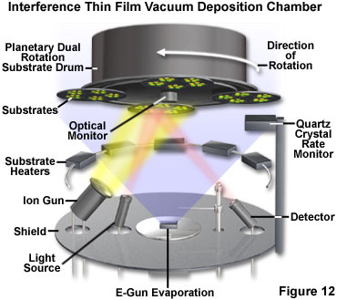
Regardless of the vapor production method for depositing thin-film coatings, certain aspects of the fabrication process are similar. A number of uncoated substrates are placed in a large chamber that is capable of achieving high vacuum (as illustrated in Figure 12). Sources for each material to be vaporized and deposited in a single production run are placed in the chamber prior to its evacuation. Multilayer coatings are generally deposited in a continuous run without opening the vacuum chamber. In most cases, the substrates are mounted on a device that allows them to be rotated in a planetary motion, which produces the most uniform exposure of each substrate to the vapor. Careful control of the source material vaporization rate and the deposition conditions, such as temperature, pressure, and source-substrate geometry, results in uniform condensation of the vapor cloud onto the rotating substrates to form a continuous thin-film coating.
As the deposition progresses, the increasing film thickness is monitored optically, and the substrates are shielded or vaporization is stopped when the precise desired optical thickness is achieved. Multilayer coatings commonly consist of as many as a hundred layers, and are produced by repeating the coating cycle with two or more materials deposited in the required sequence. The optical monitoring process utilized to control the film deposition takes advantage of the same interference characteristics for which the filter coatings are being produced. During the coating cycle, a monitor light beam of specific wavelength passes through the vacuum chamber and is incident on a blank reference substrate. Light reflected from the substrate is detected with a photomultiplier device that is phase-sensitive. As the thickness of a deposited layer on the blank substrate increases, the intensity of reflected light varies according to the nature of interference occurring among the reflected beams. The reflected intensity oscillates in an approximate sine wave pattern as the conditions for constructive and destructive interference are alternately attained. The turning points of the alternating intensity curve represent quarter-wave and half-wave optical thickness at the monitor wavelength, with those points separated by intermediate thickness values. The deposition of each layer is terminated by the monitoring circuit at the appropriate reflectance value.
Although numerous techniques have been developed for vaporizing coating materials in vacuum deposition applications, only two of these are commonly employed for fabrication of thin-film interference filters. The original method, dating back to initial development of vacuum coating technology and still widely used, relies on resistive thermal evaporation by direct heating of small folded strips (or boats) of tungsten, molybdenum, or tantalum containing the coating materials. By passing a high current through the boat, the coating material is thermally vaporized and migrates through the vacuum chamber to be re-condensed into a film on the substrates. Thermal evaporation suffers from a number of problems. The primary difficulty is the high temperature required to melt useful coating materials, which generates side reactions that result in contamination of the deposited films. Furthermore, many materials with desirable optical properties coupled with high durability and transparency are the same refractory oxides that have been historically employed in the manufacture of glass and ceramics. The high melting points of these refractory materials, particularly metal oxides, prevent them from being vaporized from metal boats, which themselves melt at lower temperatures. If limited to this evaporation technique, thin-film coatings can only be produced from materials with relatively high volatility (moderate melting points), which unfortunately exhibit rather poor durability and environmental resistance. The low resilience of these films also makes it impractical to produce complex filters requiring many coating layers.
The development of electron-beam guns for the melting or sublimation of source materials has alleviated many of the problems inherent in resistive heating technology. Electron bombardment has become the preferred method for optical thin-film production, and has made it possible to volatilize refractory metal oxides, such as silicon dioxide, aluminum and magnesium oxides, as well as transition-metal oxides, including titanium oxide and zirconium oxide. The method involves focusing a high-flux electron beam (approximately 1 ampere at 10-kilovolt potential) onto coating materials contained in large cooled crucibles. Intense localized heating and vaporization of the source materials avoids any reaction with the relatively cool crucible. Additionally, the electron gun can be focused as required to produce sufficient intensity to vaporize even substances having extremely low volatility. A further innovation that is often employed in conjunction with electron-beam melting is the introduction of a low oxygen partial pressure to the chamber during evaporation of oxide materials (termed reactive evaporation) to improve process yields.
Several fabrication techniques have been developed that enable significant improvements in the properties of thin-film coatings produced by physical vapor deposition methods. Referred to as energetic PVD processes, the most common examples are ion-assisted deposition, ion-beam sputtering, and reactive magnetron sputtering. Energetic PVD methods can, in many instances, result in fabrication of thin films with improved properties, including higher density, higher refractive index, decreased spectral performance sensitivity to temperature and moisture, and superior mechanical characteristics (such as durability).
Ion-assisted deposition is a modification of evaporation methods that utilize either direct thermal or electron-beam vaporization of source materials. The addition of an energetic ion source that bombards the substrate with ions during coating leads to increased packing density in the film layers, and an accompanying increase in refractive index and improved mechanical characteristics of the coated substrates. Reduction of voids in the more densely packed films reduces the potential for water absorption, which is a common cause of mechanical failure and changes in optical properties. Depending on the films being deposited, various ion species may be employed, including oxygen or inert gases such as argon.
In the ion-beam sputtering technique, an energetic ion source is used to bombard a metal or dielectric oxide target with high-velocity ions. Atoms of the target material are physically displaced, or sputtered, from the target surface and a portion of these are condensed into thin films on the coating substrates. A variation of the process, sometimes referred to as dual ion-beam sputtering, adds a second ion beam to bombard the films during growth with oxygen, argon, or other gases in a fashion similar to the ion-assisted bombardment sometimes utilized with evaporation techniques.
A third energetic PVD process, reactive magnetron sputtering, has been applied in the production of interference coatings. This technique has the advantage of creating films with desirable properties equivalent to those of ion-beam sputtered films, but at much higher deposition rates. Reactive magnetron sputtering employs direct current magnetron sputtering of a metal or semiconductor target to produce films that react with the substrate in forming a desired oxide layer. Variations to enhance the process have been discovered, including oxygen ion bombardment of the substrate during film growth.
A wide variety of substrate materials can be utilized for fabrication of thin-film interference filters, and are chosen to meet the optical and mechanical requirements of their intended application as well as for compatibility of their physical properties with the required coating materials. Among the properties that are significant for optical substrate materials in various applications are transmittance in the wavelength range of interest, thermal expansion coefficients, density, and resistance to laser damage. The materials should also be resistant to chemical etching, and to mechanical and thermal shock. Some of the more common optical substrate materials are magnesium fluoride, calcium fluoride, Suprasil 1 (trade name for a variety of fused silica), ultraviolet-grade fused silica, Infrasil 301 (trade name for fused natural quartz product having low hydroxyl content), crystal quartz, BK7 (a borosilicate crown optical glass), and sapphire.
Additional Considerations for Laser Scanning Confocal Systems
The implementation of scanning confocal techniques creates a number of additional requirements for optical elements utilized in fluorescence imaging, including interference filters that are part of the fluorescence set. A common misconception when laser illumination is employed is that a specific laser produces light of only one wavelength. Actually, almost every laser generates additional harmonics and light from scattering at multiple wavelengths. Although the intensities of these secondary lines are typically low relative to the principal spectral line (or lines), they can, nevertheless, severely affect the system signal-to-noise characteristics. The often-weak fluorescence signal can be completely masked by the harmonics or scattered light if the desired emission line falls in the same wavelength region as the noise. To alleviate this potential problem, a laser clean-up filter is incorporated as the first optical element in the illumination path. This filter is, in effect, a modified variation of the excitation filter, and for laser illumination, is required to be ground and polished to high optical quality. Although widefield techniques do not require the same precision in the illumination path, the clean-up filter should be polished to exhibit a transmitted wavefront distortion of less than one wavelength per inch for confocal applications.
Similarly, the wedge specification for clean-up filters should be minimized (to less than 1 arc-minute) in order to allow different filters to be used in the same beam path (for several laser lines) without realignment of the optics. This type of filter is usually fabricated with layer structure that maximizes reflection properties, in order to avoid thermal damage to the filter from intense laser radiation. The clean-up filter is then mounted at an angle of several degrees from perpendicular (with respect to the optic axis) to prevent excessive reflected light from reentering the laser cavity and producing damage that would reduce the laser life. A typical laser clean-up filter is designed to block all light from the laser source except for the passband of approximately 10 nanometers.
In confocal fluorescence applications, the dichromatic mirror or beamsplitter must also meet more stringent specifications than those required for widefield microscopy. Both the transmitted wavefront distortion and the wedge specification should not exceed one wavelength per inch. Because any optical element placed in the beam path at an angle can introduce polarization changes, this factor must also be considered for the dichromatic mirror, particularly because most laser sources are polarized. Different beamsplitter transmission or reflection profiles for the two orthogonally polarized beam components can result in an extreme situation in which light polarized in one direction is reflected, while light of the same wavelength, but polarized in the perpendicular direction, is transmitted.
The function of the emission filter in confocal fluorescence systems is equivalent to that in conventional widefield microscopy, although the excitation radiation that must be blocked occurs over a narrower spectral region. The increased power of the laser excitation lines compared to broadband illumination sources (such as a mercury arc-discharge lamp) may require filters for laser sources to be designed with more stringent blocking specifications at the principal excitation wavelengths. Emission filters are usually ground and polished to precise optical specifications for widefield microscopy, and this is generally considered appropriate for confocal imaging as well. There is some disagreement over the importance of the stringent requirements for emission filters in confocal scanning systems, which form an image pixel-by-pixel in serial fashion from a photomultiplier detector signal. Because of the high precision required to maintain confocality and exclude out-of-plane signal, the additional precision is likely to be beneficial to the extent that it limits signal distortion.
Conclusion
Many specialized microscopy techniques benefit significantly from the fact that the fundamental principles governing interference filter operation enable relatively simple and precise manipulation of the filter optical properties over a large and practical range. One of the keys to the success of interference filter technology is the versatility of the fabrication methods, which enables production of an enormous variety of filters for many applications. Once design details are established through computer modeling and simulation testing, entirely different filters can be produced, in some instances, by a manufacturing change as simple as loading different source materials into a vacuum coating system and reprogramming the coating parameters. The capability of depositing refractive-oxide materials using energetic physical vapor deposition techniques has greatly advanced the production of high-performance practical interference filters for a wide range of applications including high-resolution, high-sensitivity fluorescence microscopy.
Sorry, this page is not
available in your country.